
5SGXEA7K2F40C1G
| Part Description |
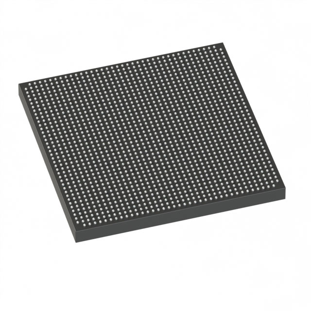
Stratix® V GX Field Programmable Gate Array (FPGA) IC 696 51200000 622000 1517-BBGA, FCBGA |
|---|---|
| Quantity | 1,116 Available (as of June 14, 2026) |

| Product Category | Field Programmable Gate Array (FPGA) |
|---|---|
| Manufacturer | Intel |
| Manufacturing Status | Active |
| Manufacturer Standard Lead Time | 26 Weeks |
| Datasheet |
Specifications & Environmental
| Device Package | 1517-FBGA (40x40) | Grade | Commercial | Operating Temperature | 0°C – 85°C | ||
|---|---|---|---|---|---|---|---|
| Package / Case | 1517-BBGA, FCBGA | Number of I/O | 696 | Voltage | 870 mV - 930 mV | ||
| Mounting Method | Surface Mount | RoHS Compliance | RoHS Compliant | REACH Compliance | REACH Unaffected | ||
| Moisture Sensitivity Level | 3 (168 Hours) | Number of LABs/CLBs | 234720 | Number of Logic Elements/Cells | 622000 | ||
| Number of Gates | N/A | ECCN | N/A | HTS Code | N/A | ||
| Qualification | N/A | Total RAM Bits | 51200000 |
Overview of 5SGXEA7K2F40C1G – Stratix® V GX Field Programmable Gate Array (FPGA) IC 696 51200000 622000 1517-BBGA, FCBGA
The 5SGXEA7K2F40C1G is a Stratix V GX family FPGA from Intel, offering a high-density programmable fabric and an extensive I/O complement in a 1517-ball FCBGA package. This commercial-grade device combines large logic capacity, substantial on-chip RAM, and a wide I/O count for complex digital, signal-processing and transceiver-aware designs.
Engineered for applications that require heavy integration of logic and memory with flexible board-level routing, the device is supplied with documented electrical and switching characteristics within the Stratix V device datasheet.
Key Features
- Logic Capacity 622,000 logic elements (cells) to support large-scale digital designs and integration of complex functions on a single device.
- Embedded Memory Approximately 51.2 Mbits of on-chip RAM for buffering, data moves, and algorithmic storage without external memory.
- I/O Resources 696 user I/Os to accommodate dense board-level interfacing and multiple parallel or serialized interfaces.
- Package & Mounting 1517-BBGA, FCBGA (supplier package: 1517-FBGA 40×40) in a surface-mount form factor to support compact, high-density PCB layouts.
- Power Core voltage supply range 0.870 V to 0.930 V to match Stratix V core power requirements as specified in device documentation.
- Temperature & Grade Commercial grade with an operating temperature range of 0 °C to 85 °C suitable for standard commercial environments.
- Compliance RoHS compliant, meeting common material and environmental regulatory requirements.
Typical Applications
- High‑density logic integration Implements large, custom digital systems that require significant on-chip logic and memory resources.
- Transceiver‑aware systems Ideal for designs that leverage Stratix V GX transceiver capabilities and detailed I/O timing documented in the device datasheet.
- Data buffering and on‑chip storage Uses the device’s embedded RAM for packet buffering, FIFOs, or intermediate storage in signal-processing pipelines.
- Dense I/O applications Suits designs needing hundreds of user I/Os for parallel interfaces, wide buses, or multiple interface types.
Unique Advantages
- High logic density: 622,000 logic elements enable consolidation of multiple functions into a single FPGA, reducing board-level component count.
- Large on‑chip memory: Approximately 51.2 Mbits of embedded RAM reduces dependence on external memory for many buffering and data-processing tasks.
- Extensive I/O: 696 I/Os provide flexibility for complex system interfaces, facilitating integration with diverse peripherals and subsystems.
- Compact package: 1517-ball FCBGA (40×40) supports high connection density in space-constrained designs while maintaining surface-mount assembly compatibility.
- Commercial operating range: 0 °C to 85 °C and defined core supply range simplify thermal and power budgeting for mainstream electronic systems.
- Regulatory compliance: RoHS compliance helps meet material restrictions for commercial product deployment.
Why Choose 5SGXEA7K2F40C1G?
The 5SGXEA7K2F40C1G delivers a combination of large logic capacity, significant embedded memory, and broad I/O resources in a compact FCBGA package—making it well suited for designers who need to integrate complex digital functions and substantial on‑chip data storage. As a member of the Stratix V GX family, its electrical and switching characteristics are documented in the Stratix V device datasheet for design planning and verification.
This device is a practical choice for engineering teams building commercial-grade systems that require high integration density, flexible interfacing, and controlled power and thermal parameters consistent with the provided specifications.
Request a quote or submit an inquiry to receive pricing and availability information for the 5SGXEA7K2F40C1G.


Date Founded: 1968
Headquarters: Santa Clara, California, USA
Employees: 130,000+
Revenue: $54.23 Billion
Certifications and Memberships: ISO9001:2015, ISO14001:2015, ISO17025:2017, ISO27001:2022, ISO45001:2018, ISO50001:2018


