
5SGXEA7K2F35I3LG
| Part Description |
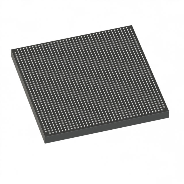
Stratix® V GX Field Programmable Gate Array (FPGA) IC 432 51200000 622000 1152-BBGA, FCBGA |
|---|---|
| Quantity | 681 Available (as of June 15, 2026) |

| Product Category | Field Programmable Gate Array (FPGA) |
|---|---|
| Manufacturer | Intel |
| Manufacturing Status | Active |
| Manufacturer Standard Lead Time | 26 Weeks |
| Datasheet |
Specifications & Environmental
| Device Package | 1152-FBGA (35x35) | Grade | Industrial | Operating Temperature | -40°C – 100°C | ||
|---|---|---|---|---|---|---|---|
| Package / Case | 1152-BBGA, FCBGA | Number of I/O | 432 | Voltage | 820 mV - 880 mV | ||
| Mounting Method | Surface Mount | RoHS Compliance | RoHS Compliant | REACH Compliance | REACH Unaffected | ||
| Moisture Sensitivity Level | 3 (168 Hours) | Number of LABs/CLBs | 234720 | Number of Logic Elements/Cells | 622000 | ||
| Number of Gates | N/A | ECCN | N/A | HTS Code | N/A | ||
| Qualification | N/A | Total RAM Bits | 51200000 |
Overview of 5SGXEA7K2F35I3LG – Stratix® V GX FPGA, 622,000 logic elements
The 5SGXEA7K2F35I3LG is a Stratix V GX field programmable gate array (FPGA) packaged in a 1152‑ball BGA (35×35 mm) and rated for industrial temperature operation. It provides an exceptionally large logic capacity and embedded memory with a broad I/O complement for complex digital designs.
Targeted at designs that require large programmable logic resources, significant on‑chip RAM, and a high pin count, this device delivers integration suited to demanding communications, compute and data‑processing applications while operating from a low core voltage.
Key Features
- Logic Capacity — 622,000 logic elements to implement large-scale digital systems and custom accelerators.
- Logic Array Blocks — 234,720 logic array blocks (LABs) for modular logic instantiation and hierarchical designs.
- Embedded Memory — approximately 51.2 Mbits of embedded memory for high‑bandwidth buffering, large FIFOs, and on‑chip data storage.
- I/O Resources — 432 device I/Os to interface with high‑pin‑count systems and dense mezzanine or daughtercard architectures.
- Packaging — 1152‑BBGA (FCBGA) supplier package 1152‑FBGA (35×35) for compact, high‑pin‑count PCB layouts.
- Power — core supply voltage range of 820 mV to 880 mV enabling operation at specified core rails.
- Temperature Grade — Industrial grade operation from −40 °C to 100 °C for robust deployment in constrained thermal environments.
- Stratix V GX Transceiver Capability — Stratix V GX family transceiver speed grades include support up to 14.1 Gbps (per Stratix V device datasheet).
- Regulatory — RoHS compliant.
Typical Applications
- High‑density digital processing — Use the large logic and embedded memory resources to implement custom datapaths, hardware accelerators, and complex state machines.
- Networking and communications — Leverage the Stratix V GX transceiver speed grades and abundant I/O for packet processing, PHY interfacing, and protocol bridging.
- Data acquisition and aggregation — High I/O count and sizeable on‑chip RAM enable input fan‑in, buffering, and aggregation of multi‑channel data streams.
- Signal processing and compute offload — Implement FPGA-based DSP chains and parallel compute kernels using extensive logic and memory resources.
Unique Advantages
- Massive programmable capacity: 622,000 logic elements provide the headroom for large designs and system consolidation onto a single device.
- Significant embedded memory: Approximately 51.2 Mbits of on‑chip RAM reduces reliance on external memory for buffering and accelerates data‑intensive tasks.
- High I/O count in a compact package: 432 I/Os in a 1152‑ball FCBGA (35×35) package enables dense system integration without sacrificing board real estate.
- Industrial temperature rating: −40 °C to 100 °C operation supports designs that require extended temperature range robustness.
- Low‑voltage core operation: Core supply between 820 mV and 880 mV aligns with low‑voltage system designs and power management strategies.
- Standards‑aligned family performance: Stratix V GX family transceiver grades documented in the Stratix V datasheet support multiple high‑speed link options.
Why Choose 5SGXEA7K2F35I3LG?
The 5SGXEA7K2F35I3LG combines a very large logic element count, substantial embedded memory, and a broad I/O complement in a single industrial‑grade Stratix V GX FPGA package. Its low core voltage operating window and documented transceiver grade options make it appropriate for designs that require dense integration, significant on‑chip storage, and high‑speed serial capability.
This device suits engineering teams building complex communications, signal‑processing, or compute‑accelerator systems that benefit from the Stratix V family documentation and device characteristics. Its combination of capacity, I/O density, and temperature rating supports scalable, long‑lived deployments.
Request a quote or submit a pricing request to check availability and obtain configuration and purchasing details for 5SGXEA7K2F35I3LG.


Date Founded: 1968
Headquarters: Santa Clara, California, USA
Employees: 130,000+
Revenue: $54.23 Billion
Certifications and Memberships: ISO9001:2015, ISO14001:2015, ISO17025:2017, ISO27001:2022, ISO45001:2018, ISO50001:2018


