
5SGXEA7K2F40C1
| Part Description |
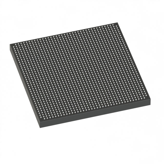
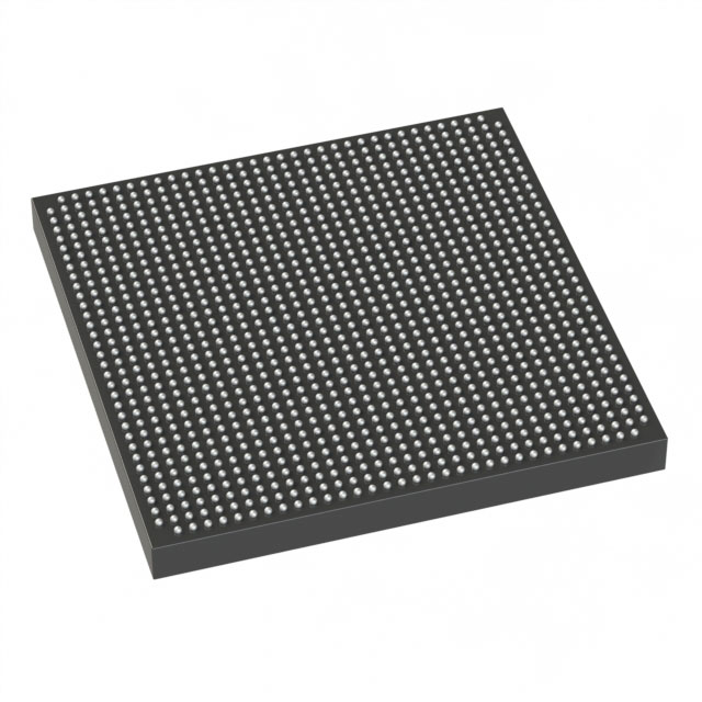
Stratix® V GX Field Programmable Gate Array (FPGA) IC 696 51200000 622000 1517-BBGA, FCBGA |
|---|---|
| Quantity | 187 Available (as of June 10, 2026) |

| Product Category | Field Programmable Gate Array (FPGA) |
|---|---|
| Manufacturer | Intel |
| Manufacturing Status | Obsolete |
| Manufacturer Standard Lead Time | Contact Us |
| Datasheet |
Specifications & Environmental
| Device Package | 1517-FBGA (40x40) | Grade | Commercial | Operating Temperature | 0°C – 85°C | ||
|---|---|---|---|---|---|---|---|
| Package / Case | 1517-BBGA, FCBGA | Number of I/O | 696 | Voltage | 870 mV - 930 mV | ||
| Mounting Method | Surface Mount | RoHS Compliance | RoHS non-compliant | REACH Compliance | REACH Unknown | ||
| Moisture Sensitivity Level | 3 (168 Hours) | Number of LABs/CLBs | 234720 | Number of Logic Elements/Cells | 622000 | ||
| Number of Gates | N/A | ECCN | 3A001A7A | HTS Code | 8542.39.0001 | ||
| Qualification | N/A | Total RAM Bits | 51200000 |
Overview of 5SGXEA7K2F40C1 – Stratix® V GX FPGA (1517-FBGA)
The 5SGXEA7K2F40C1 is an Intel Stratix V GX field-programmable gate array (FPGA) supplied in a 1517-FBGA (40×40) package. It is built on the Stratix V family architecture and targets bandwidth- and data-intensive applications requiring high logic capacity, plentiful I/O, and integrated transceiver capability.
As part of the Stratix V family, this GX variant benefits from the family’s enhanced core architecture, embedded hard IP blocks, and integrated high-speed transceivers. Typical use cases include high-bandwidth transport, packet processing, and high-performance DSP systems.
Key Features
- High Logic Capacity — Contains 622,000 logic elements for complex FPGA designs and large-scale integration.
- Embedded Memory — Approximately 51.2 Mbits of on-chip RAM, supported by Stratix V M20K 20-Kbit memory blocks for dense buffering and storage.
- I/O and Package — Up to 696 user I/O pins in a 1517-BBGA (FCBGA) 1517-FBGA (40×40) surface-mount package to support broad interfacing needs.
- Integrated Transceivers (GX) — Stratix V GX devices offer up to 66 integrated transceivers with 14.1-Gbps data-rate capability for backplane and optical interfaces.
- Core and Process — Built on a 28-nm TSMC process with supported core voltages of 0.85 V or 0.9 V; the device data lists an operating supply range of 870 mV to 930 mV.
- DSP and Fabric Building Blocks — Includes variable-precision DSP blocks, redesigned adaptive logic modules (ALMs), fractional PLLs, and a comprehensive fabric clocking and routing architecture.
- Embedded Hard IP — Features an Embedded HardCopy Block for hardened IP instantiation (for example, PCIe Gen1/Gen2/Gen3 in Stratix V family documentation).
- Power and Environmental — Surface-mount package, RoHS compliant, and specified for commercial operating temperatures from 0 °C to 85 °C.
Typical Applications
- 40G/100G Optical Transport — High-density logic and integrated transceivers enable optical transport line cards and interface modules.
- Packet Processing and Traffic Management — Large logic and abundant I/O support complex packet processing, switching, and traffic-management functions.
- High-Performance DSP — Variable-precision DSP blocks and substantial on-chip RAM make the device suitable for DSP-heavy workloads and signal-processing pipelines.
- Network Test and Measurement — Integrated transceivers and high I/O count support test equipment and backplane-based measurement systems.
Unique Advantages
- High integration and density: 622,000 logic elements and abundant embedded memory reduce the need for external logic and memory, simplifying system design.
- Built for bandwidth: Up to 66 GX transceivers at 14.1 Gbps support demanding high-speed serial links without external PHYs.
- Family-level hard IP: The Embedded HardCopy Block and family hard-IP capabilities help accelerate deployment of standards-based interfaces.
- Flexible fabric: ALMs, fractional PLLs, and multi-track routing provide a versatile architecture for varied timing and logic partitioning requirements.
- Commercial-grade readiness: RoHS-compliant, surface-mount 1517-FBGA package and a 0 °C to 85 °C operating range for typical commercial deployments.
Why Choose 5SGXEA7K2F40C1?
The 5SGXEA7K2F40C1 combines high logic capacity, substantial on-chip memory, and integrated high-speed transceivers within the Stratix V GX family architecture. It is suited for designers tackling bandwidth-centric, data-intensive, and DSP-focused applications that require a dense, programmable fabric with native transceiver support.
This device offers a clear upgrade path within the Stratix V family and benefits from family-level hard IP and fabric features, making it a practical choice for system designers seeking a high-density, commercial-grade FPGA solution.
Request a quote or submit an inquiry to receive pricing, availability, and support information for the 5SGXEA7K2F40C1.


Date Founded: 1968
Headquarters: Santa Clara, California, USA
Employees: 130,000+
Revenue: $54.23 Billion
Certifications and Memberships: ISO9001:2015, ISO14001:2015, ISO17025:2017, ISO27001:2022, ISO45001:2018, ISO50001:2018


