
5SGXEA7K2F40I3WN
| Part Description |
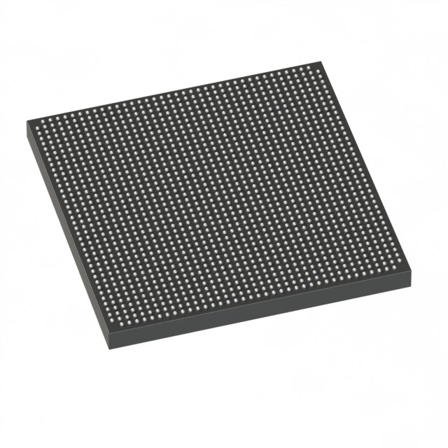
Stratix® V GX Field Programmable Gate Array (FPGA) IC 696 51200000 622000 1517-BBGA, FCBGA |
|---|---|
| Quantity | 291 Available (as of June 15, 2026) |

| Product Category | Field Programmable Gate Array (FPGA) |
|---|---|
| Manufacturer | Intel |
| Manufacturing Status | Obsolete |
| Manufacturer Standard Lead Time | Contact Us |
| Datasheet |
Specifications & Environmental
| Device Package | 1517-FBGA (40x40) | Grade | Industrial | Operating Temperature | -40°C – 100°C | ||
|---|---|---|---|---|---|---|---|
| Package / Case | 1517-BBGA, FCBGA | Number of I/O | 696 | Voltage | 820 mV - 880 mV | ||
| Mounting Method | Surface Mount | RoHS Compliance | RoHS non-compliant | REACH Compliance | REACH Unknown | ||
| Moisture Sensitivity Level | 4 (72 Hours) | Number of LABs/CLBs | 234720 | Number of Logic Elements/Cells | 622000 | ||
| Number of Gates | N/A | ECCN | OBSOLETE | HTS Code | N/A | ||
| Qualification | N/A | Total RAM Bits | 51200000 |
Overview of 5SGXEA7K2F40I3WN – Stratix® V GX FPGA, 696 I/O, 1517-BBGA
The 5SGXEA7K2F40I3WN is a Stratix® V GX field programmable gate array (FPGA) IC engineered for designs that require very large logic capacity, abundant I/O, and significant on-chip memory. It integrates 622,000 logic elements and approximately 51.2 Mbits of embedded memory to address complex digital processing tasks.
Built and specified for industrial use, this surface-mount FCBGA device provides a broad operating range and a compact 1517-BBGA package footprint, making it suitable for industrial communication, high-density signal processing, and advanced embedded systems that demand robust thermal and voltage operating margins.
Key Features
- Logic Capacity — 622,000 logic elements to implement large-scale digital designs and complex algorithmic functions.
- Embedded Memory — Approximately 51.2 Mbits of on-chip RAM for buffering, look-up tables, and data-path storage.
- I/O Density — 696 device I/Os to support wide parallel interfaces, high-pin-count connectivity, and flexible board integration.
- Power and Core Voltage — Core supply specified from 820 mV to 880 mV, enabling integration into systems designed around low-voltage FPGA cores.
- Industrial Temperature Grade — Rated for operation from −40 °C to 100 °C for deployment in industrial environments.
- Package and Mounting — 1517-BBGA, FCBGA package (supplier device package: 1517-FBGA, 40×40) in a surface-mount form factor for compact PCB designs.
- RoHS Compliant — Meets RoHS environmental requirements.
Typical Applications
- High-density digital signal processing — Implements large DSP chains and parallel processing engines leveraging the device's logic and memory resources.
- Industrial control and automation — Supports complex control algorithms and extensive I/O counts within industrial temperature ranges.
- Network and communications infrastructure — Provides the logic capacity and I/O required for packet processing, protocol handling, and custom interface bridging.
- Advanced embedded systems — Enables system-level integration where on-chip memory and high logic counts reduce external component requirements.
Unique Advantages
- Large on-chip logic pool: 622,000 logic elements allow integration of complex functions that would otherwise require multiple devices, reducing system BOM and board complexity.
- Substantial embedded memory: Approximately 51.2 Mbits of RAM provides on-chip buffering and storage for high-throughput processing and reduced external memory dependence.
- High I/O count: 696 I/Os enable wide parallel interfaces and flexible connectivity options for multi-channel systems.
- Industrial-grade thermal range: Rated from −40 °C to 100 °C for reliable operation in harsh or temperature-variable environments.
- Compact FCBGA package: The 1517-BBGA (1517-FBGA, 40×40) package delivers high density in a surface-mount form factor suitable for space-constrained PCBs.
- Low-voltage core operation: Core supply range of 820 mV–880 mV aligns with low-voltage FPGA system designs.
Why Choose 5SGXEA7K2F40I3WN?
The 5SGXEA7K2F40I3WN places substantial programmable resources—622,000 logic elements and approximately 51.2 Mbits of embedded memory—into a single industrial-grade FCBGA package with 696 I/Os. Its combination of logic density, on-chip memory, and high I/O count makes it well suited to designs that demand integration, parallel processing, and robust thermal performance.
For engineering teams building complex industrial, communication, or high-performance embedded systems, this Stratix V GX device provides a scalable platform that reduces external component needs and supports long-term design stability backed by the Stratix V device family specifications.
Request a quote or submit your design requirements to obtain pricing and availability for the 5SGXEA7K2F40I3WN.


Date Founded: 1968
Headquarters: Santa Clara, California, USA
Employees: 130,000+
Revenue: $54.23 Billion
Certifications and Memberships: ISO9001:2015, ISO14001:2015, ISO17025:2017, ISO27001:2022, ISO45001:2018, ISO50001:2018


