
5SGXEA7K3F35C2G
| Part Description |
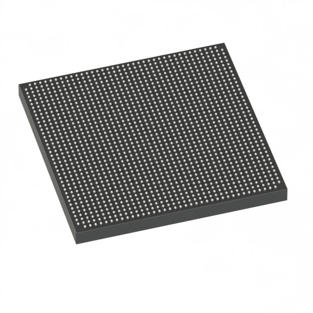
Stratix® V GX Field Programmable Gate Array (FPGA) IC 432 51200000 622000 1152-BBGA, FCBGA |
|---|---|
| Quantity | 73 Available (as of June 14, 2026) |

| Product Category | Field Programmable Gate Array (FPGA) |
|---|---|
| Manufacturer | Intel |
| Manufacturing Status | Active |
| Manufacturer Standard Lead Time | 26 Weeks |
| Datasheet |
Specifications & Environmental
| Device Package | 1152-FBGA (35x35) | Grade | Commercial | Operating Temperature | 0°C – 85°C | ||
|---|---|---|---|---|---|---|---|
| Package / Case | 1152-BBGA, FCBGA | Number of I/O | 432 | Voltage | 870 mV - 930 mV | ||
| Mounting Method | Surface Mount | RoHS Compliance | RoHS Compliant | REACH Compliance | REACH Unaffected | ||
| Moisture Sensitivity Level | 3 (168 Hours) | Number of LABs/CLBs | 234720 | Number of Logic Elements/Cells | 622000 | ||
| Number of Gates | N/A | ECCN | N/A | HTS Code | N/A | ||
| Qualification | N/A | Total RAM Bits | 51200000 |
Overview of 5SGXEA7K3F35C2G – Stratix® V GX Field Programmable Gate Array (FPGA) IC 432 51200000 622000 1152-BBGA, FCBGA
The 5SGXEA7K3F35C2G is a Stratix V GX Field Programmable Gate Array (FPGA) from Intel, supplied in a 1152‑ball FCBGA package. It delivers very high logic capacity and on‑chip memory with a substantial I/O complement for complex, programmable digital designs.
As a commercial‑grade Stratix V GX device, it targets systems that require high logic density, abundant embedded memory, and multi‑lane serial connectivity options supported across the Stratix V family.
Key Features
- High Logic Density Provides 622,000 logic elements to implement large-scale programmable logic and custom datapaths.
- Embedded Memory Approximately 51 Mbits of on‑chip RAM (51,200,000 bits) to support buffering, lookup tables, and state storage without external memory.
- I/O Capacity 432 I/O pins for broad peripheral and board‑level interfacing options.
- Transceiver Capability (Stratix V GX family) Stratix V GX devices are offered with multiple transceiver speed grades; the family supports GX channel speeds up to 14.1 Gbps according to the device datasheet.
- Package & Mounting 1152‑BBGA (FCBGA) package; supplier device package listed as 1152‑FBGA (35×35). Surface mount device suitable for standard PCB assembly.
- Power Supply Range Operates with a specified supply range of 870 mV to 930 mV.
- Commercial Temperature Grade Rated for commercial operation from 0 °C to 85 °C.
- Regulatory RoHS compliant.
Typical Applications
- High‑density programmable logic Large logic capacity and abundant on‑chip RAM make this device suitable for complex state machines, custom accelerators, and large FPGA designs.
- High‑speed serial I/O systems Stratix V GX transceiver speed grades in the family support multi‑Gbps channels for serial connectivity and protocol bridging tasks.
- Multi‑interface aggregation High I/O count enables bridging and aggregation of numerous board‑level interfaces and peripherals.
Unique Advantages
- Substantial logic resources: 622,000 logic elements reduce the need to partition designs across multiple devices.
- Large on‑chip memory: Approximately 51 Mbits of embedded RAM lowers external memory dependence for many buffering and table look‑up needs.
- High I/O density: 432 I/O pins provide flexibility for dense board‑level connectivity and multiple peripheral interfaces.
- Family transceiver options: As a Stratix V GX part, the device is part of a family that supports high‑speed transceiver speed grades up to 14.1 Gbps per the datasheet.
- Compact FCBGA package: 1152‑ball FCBGA (35×35) provides a compact footprint for high‑performance FPGA integration on space‑constrained PCBs.
- Commercial readiness: Commercial temperature rating (0 °C to 85 °C) and RoHS compliance support mainstream electronic product deployments.
Why Choose 5SGXEA7K3F35C2G?
The 5SGXEA7K3F35C2G combines very high logic capacity, substantial embedded memory, and a large I/O set in a compact 1152‑ball FCBGA package. It is well suited for designers who need to consolidate complex digital functions, large state machines, and high‑bandwidth I/O into a single commercial‑grade FPGA.
Choosing this Stratix V GX device provides a scalable platform within the Stratix V family, leveraging multi‑Gbps transceiver speed grade options and a proven datasheet foundation to support demanding, programmable system designs.
Request a quote or submit an inquiry to receive pricing, availability, and technical support information for 5SGXEA7K3F35C2G.


Date Founded: 1968
Headquarters: Santa Clara, California, USA
Employees: 130,000+
Revenue: $54.23 Billion
Certifications and Memberships: ISO9001:2015, ISO14001:2015, ISO17025:2017, ISO27001:2022, ISO45001:2018, ISO50001:2018


