
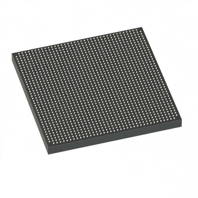
5SGXEA7K3F35C2LG
| Part Description |
Stratix® V GX Field Programmable Gate Array (FPGA) IC 432 51200000 622000 1152-BBGA, FCBGA |
|---|---|
| Quantity | 566 Available (as of June 15, 2026) |

| Product Category | Field Programmable Gate Array (FPGA) |
|---|---|
| Manufacturer | Intel |
| Manufacturing Status | Active |
| Manufacturer Standard Lead Time | 26 Weeks |
| Datasheet |
Specifications & Environmental
| Device Package | 1152-FBGA (35x35) | Grade | Commercial | Operating Temperature | 0°C – 85°C | ||
|---|---|---|---|---|---|---|---|
| Package / Case | 1152-BBGA, FCBGA | Number of I/O | 432 | Voltage | 820 mV - 880 mV | ||
| Mounting Method | Surface Mount | RoHS Compliance | RoHS Compliant | REACH Compliance | REACH Unaffected | ||
| Moisture Sensitivity Level | 3 (168 Hours) | Number of LABs/CLBs | 234720 | Number of Logic Elements/Cells | 622000 | ||
| Number of Gates | N/A | ECCN | N/A | HTS Code | N/A | ||
| Qualification | N/A | Total RAM Bits | 51200000 |
Overview of 5SGXEA7K3F35C2LG – Stratix® V GX FPGA, 432 I/Os, approximately 622,000 logic elements, 1152‑BBGA
The 5SGXEA7K3F35C2LG is a Stratix® V GX field programmable gate array (FPGA) in a 1152‑ball BGA (FCBGA) package. It delivers very high logic capacity and on‑chip memory while providing a large number of I/O pins for complex, I/O‑intensive commercial designs.
Targeted at commercial applications that require high-density programmable logic and abundant embedded memory, this device offers integration and scalability for systems that demand large logic counts, substantial embedded RAM, and extensive I/O connectivity.
Key Features
- High Logic Capacity Approximately 622,000 logic elements to implement large, complex digital designs.
- Embedded Memory Approximately 51.2 Mbits of on‑chip RAM for buffering, packet processing, and state storage.
- Logic Fabric Scale 234,720 LABs/CLBs (family layout metric) to organize and map high‑density logic and routing.
- Abundant I/O 432 I/O pins to support wide parallel interfaces, multi‑lane connectivity, and diverse I/O standards (package I/O count as specified).
- Power and Core Supply Core operating voltage range of 820 mV to 880 mV for the device core supply requirements.
- Commercial Temperature Grade Rated for 0 °C to 85 °C operation for commercial environments.
- Package and Mounting 1152‑BBGA (FCBGA) package; supplier device package listed as 1152‑FBGA (35×35); surface mount mounting type.
- RoHS Compliant Manufactured to comply with RoHS requirements.
- Series Transceiver Capability (Stratix V GX family) Stratix V GX family transceivers are described in the device series documentation with transceiver speed grades up to 14.1 Gbps (series‑level capability described in the Stratix V device datasheet).
Typical Applications
- High‑density digital systems Implement large custom logic blocks, datapaths, and state machines where extensive logic resources and embedded RAM are required.
- I/O‑intensive designs Support systems that need many parallel interfaces or multiple high‑pin-count peripherals through its 432 I/O pins.
- Packet and data buffering Use embedded RAM for buffering, queues, and line‑rate data handling in commercial networking or communications equipment.
- Prototyping and system integration Leverage the device’s logic density and package options for prototyping high‑capacity FPGA designs in commercial product development.
Unique Advantages
- Large programmable fabric: Approximately 622,000 logic elements reduce the need to partition designs across multiple devices, simplifying board and system design.
- Significant on‑chip memory: Around 51.2 Mbits of embedded RAM enables local buffering and state retention without external memory for many use cases.
- Extensive I/O availability: 432 I/Os provide flexibility to interface with multiple peripherals, parallel buses, and multi‑lane I/O schemes.
- Commercial readiness: Rated for commercial temperature range (0 °C to 85 °C) and RoHS compliant to meet typical commercial product requirements.
- Compact, assembly‑friendly package: 1152‑ball FCBGA package in a 35×35 outline supports surface‑mount assembly for space‑constrained PCBs.
Why Choose 5SGXEA7K3F35C2LG?
5SGXEA7K3F35C2LG combines high logic density, substantial embedded memory, and a large I/O count in a single commercial‑grade Stratix V GX package. It is intended for designers who need a highly integrated FPGA solution to consolidate complex digital functions, reduce BOM complexity, and support I/O‑heavy applications.
This device suits teams developing commercial electronics that require scalability and robust on‑chip resources. The Stratix V series documentation provides further series‑level capabilities for transceivers and speed grades to inform system‑level planning and integration.
If you would like pricing, availability, or technical procurement details for 5SGXEA7K3F35C2LG, submit a request for a quote or pricing inquiry to evaluate this Stratix V GX FPGA for your design.


Date Founded: 1968
Headquarters: Santa Clara, California, USA
Employees: 130,000+
Revenue: $54.23 Billion
Certifications and Memberships: ISO9001:2015, ISO14001:2015, ISO17025:2017, ISO27001:2022, ISO45001:2018, ISO50001:2018


