
5SGXEA9N2F45C2LG
| Part Description |
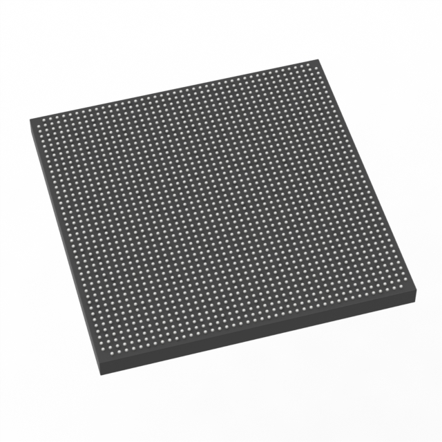
Stratix® V GX Field Programmable Gate Array (FPGA) IC 840 53248000 840000 1932-BBGA, FCBGA |
|---|---|
| Quantity | 883 Available (as of June 15, 2026) |
| Product Category | Field Programmable Gate Array (FPGA) |
|---|---|
| Manufacturer | Intel |
| Manufacturing Status | Active |
| Manufacturer Standard Lead Time | 26 Weeks |
| Datasheet |
Specifications & Environmental
| Device Package | 1932-FBGA, FC (45x45) | Grade | Commercial | Operating Temperature | 0°C – 85°C | ||
|---|---|---|---|---|---|---|---|
| Package / Case | 1932-BBGA, FCBGA | Number of I/O | 840 | Voltage | 820 mV - 880 mV | ||
| Mounting Method | Surface Mount | RoHS Compliance | RoHS Compliant | REACH Compliance | REACH Unaffected | ||
| Moisture Sensitivity Level | 3 (168 Hours) | Number of LABs/CLBs | 317000 | Number of Logic Elements/Cells | 840000 | ||
| Number of Gates | N/A | ECCN | N/A | HTS Code | N/A | ||
| Qualification | N/A | Total RAM Bits | 53248000 |
Overview of 5SGXEA9N2F45C2LG – Stratix® V GX Field Programmable Gate Array (FPGA) IC
The 5SGXEA9N2F45C2LG is a Stratix® V GX family FPGA featuring a high-capacity programmable fabric and large on-chip memory. This commercial-grade, surface-mount device provides design teams with substantial logic resources, dense I/O, and a compact FCBGA package for high-density board integration.
Key silicon characteristics include 840,000 logic elements and approximately 53 Mbits of embedded RAM, making the device suitable for complex digital designs that require large logic capacity and significant embedded memory.
Key Features
- Core Logic Capacity 840,000 logic elements for large-scale, highly parallel digital implementations.
- Embedded Memory Approximately 53 Mbits of on-chip RAM to support buffers, FIFOs, and memory-intensive algorithms.
- I/O Density Up to 840 I/O pins to accommodate wide parallel interfaces and multiple external peripherals.
- Package 1932-BBGA, FCBGA package (supplier device package listed as 1932-FBGA, FC (45×45)) for compact, high-pin-count board designs.
- Power and Voltage Core supply voltage range of 820 mV to 880 mV to match system power delivery requirements.
- Thermal & Grade Commercial temperature grade with an operating range of 0 °C to 85 °C.
- Mounting Surface mount device optimized for modern PCB assembly processes.
- Environmental Compliance RoHS compliant.
Typical Applications
- High-performance signal processing Leverage 840,000 logic elements and large embedded RAM to implement complex DSP pipelines, filters, and accelerators.
- Communications and networking Dense I/O and large logic capacity support packet processing, protocol offload, and custom network functions.
- Prototyping and system integration High fabric density and substantial memory make this device suitable for prototyping large SoC functions and integration of multiple IP blocks.
- Data-path acceleration On-chip RAM and extensive logic resources enable buffering, parallel processing, and custom hardware acceleration engines.
Unique Advantages
- High fabric capacity: 840,000 logic elements provide significant headroom for large designs and parallel architectures.
- Substantial embedded memory: Approximately 53 Mbits of on-chip RAM reduces external memory dependency for many buffering and stateful operations.
- Extensive I/O footprint: 840 I/O pins enable broad connectivity for multi-channel interfaces and high-pin-count peripherals.
- Compact high-pin package: 1932-BBGA (FCBGA) in a 45×45 supplier package balances pin count and PCB area for dense system designs.
- Low-voltage core operation: 820–880 mV core supply range aligns with modern power-optimized system architectures.
- Commercial temperature and RoHS compliance: Designed for commercial deployments with environmental compliance for regulated markets.
Why Choose 5SGXEA9N2F45C2LG?
The 5SGXEA9N2F45C2LG delivers a combination of very high logic density, large embedded RAM, and extensive I/O in a compact FCBGA package—targeted at designers who need substantial on-chip resources for complex digital, networking, or acceleration tasks. Its commercial-grade temperature range and RoHS compliance make it suitable for standard industrial and enterprise applications where high integration and strong memory resources are required.
This part is ideal for engineering teams developing large-scale FPGA designs that require scalable logic capacity and significant on-chip memory while maintaining a compact board footprint and modern low-voltage core operation.
Request a quote or submit an inquiry to receive pricing and availability details for the 5SGXEA9N2F45C2LG. Our team can provide lead-time information and assist with volume and procurement questions.


Date Founded: 1968
Headquarters: Santa Clara, California, USA
Employees: 130,000+
Revenue: $54.23 Billion
Certifications and Memberships: ISO9001:2015, ISO14001:2015, ISO17025:2017, ISO27001:2022, ISO45001:2018, ISO50001:2018


