
5SGXEA9N2F45I2LG
| Part Description |
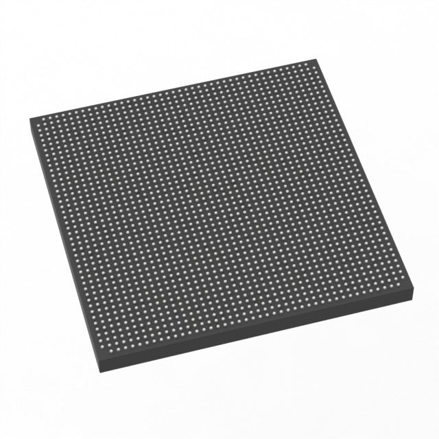
Stratix® V GX Field Programmable Gate Array (FPGA) IC 840 53248000 840000 1932-BBGA, FCBGA |
|---|---|
| Quantity | 28 Available (as of June 15, 2026) |

| Product Category | Field Programmable Gate Array (FPGA) |
|---|---|
| Manufacturer | Intel |
| Manufacturing Status | Active |
| Manufacturer Standard Lead Time | 26 Weeks |
| Datasheet |
Specifications & Environmental
| Device Package | 1932-FBGA, FC (45x45) | Grade | Industrial | Operating Temperature | -40°C – 100°C | ||
|---|---|---|---|---|---|---|---|
| Package / Case | 1932-BBGA, FCBGA | Number of I/O | 840 | Voltage | 820 mV - 880 mV | ||
| Mounting Method | Surface Mount | RoHS Compliance | RoHS Compliant | REACH Compliance | REACH Unaffected | ||
| Moisture Sensitivity Level | 3 (168 Hours) | Number of LABs/CLBs | 317000 | Number of Logic Elements/Cells | 840000 | ||
| Number of Gates | N/A | ECCN | N/A | HTS Code | N/A | ||
| Qualification | N/A | Total RAM Bits | 53248000 |
Overview of 5SGXEA9N2F45I2LG – Stratix® V GX FPGA, 840,000 logic elements, ~53.25 Mbits embedded RAM
The 5SGXEA9N2F45I2LG is a Stratix® V GX Field Programmable Gate Array (FPGA) in an industrial temperature grade, designed for high-density programmable logic applications. It combines a large logic fabric with substantial on-chip memory and a high I/O count to support complex, I/O‑intensive designs.
Built for surface-mount deployment in a 1932-BBGA (FCBGA) package, this device provides a compact, high-pin-count option where robust operating range and scalability of programmable logic resources are required.
Key Features
- Core Logic 840,000 logic elements to implement large-scale digital designs and custom logic functions.
- Embedded Memory Approximately 53.25 Mbits of on-chip RAM to support buffering, look-up tables, and data-intensive processing close to the fabric.
- I/O Capacity 840 I/O to accommodate high fanout interfaces, parallel buses, and multi-channel connectivity.
- Power and Voltage Core supply voltage range of 820 mV to 880 mV for defined power-domain planning and supply sequencing.
- Package & Mounting 1932-BBGA, FCBGA (supplier package: 1932-FBGA, FC 45×45) in a surface-mount form factor for dense board-level integration.
- Temperature & Grade Industrial grade with an operating temperature range of −40 °C to 100 °C for deployment in demanding environments.
- Standards Compliance RoHS compliant to support regulatory and environmental requirements.
Typical Applications
- High-density signal processing — Leverage 840,000 logic elements and substantial embedded RAM for FPGA-based DSP pipelines and custom accelerators.
- Multi‑channel I/O hubs — Use 840 I/O to aggregate and route parallel interfaces, bridging multiple peripherals or sensor arrays.
- Industrial control and automation — Industrial temperature rating (−40 °C to 100 °C) and high I/O enable real-time control, motor drives, and factory instrumentation.
- Prototype and system integration — High logic density and on-chip memory make the device suitable for complex prototypes and consolidated system functions on a single FPGA.
Unique Advantages
- Large programmable fabric: 840,000 logic elements allow implementation of extensive custom logic without partitioning across multiple devices.
- On‑chip memory for latency‑sensitive tasks: Approximately 53.25 Mbits of embedded RAM reduces external memory dependence and improves data-path performance.
- High I/O count: 840 I/O simplifies board-level routing for multi-channel systems and dense connector interfaces.
- Industrial operating range: −40 °C to 100 °C supports deployments in temperature-challenging environments.
- Compact, high‑pin package: 1932-BBGA (45×45 mm footprint) delivers high pin density while maintaining a surface-mount profile for modern PCB assembly.
- RoHS compliant: Aligns with environmental and manufacturing process requirements.
Why Choose 5SGXEA9N2F45I2LG?
The 5SGXEA9N2F45I2LG positions itself as a high-density, industrial-grade Stratix V GX FPGA option for engineers who need substantial logic capacity, large embedded memory, and extensive I/O in a compact surface-mount package. Its defined core voltage range and operating temperature make it suitable for robust system designs that require long-term stability and deterministic on-chip resources.
This device is appropriate for development teams targeting consolidation of complex functions onto a single FPGA, reducing board-level complexity while retaining flexibility for future reconfiguration.
Request a quote or submit an inquiry to discuss pricing, lead time, and integration details for the 5SGXEA9N2F45I2LG. Our team can provide availability and ordering information to support your project schedule.


Date Founded: 1968
Headquarters: Santa Clara, California, USA
Employees: 130,000+
Revenue: $54.23 Billion
Certifications and Memberships: ISO9001:2015, ISO14001:2015, ISO17025:2017, ISO27001:2022, ISO45001:2018, ISO50001:2018


