
5SGXEABK1H40C2G
| Part Description |
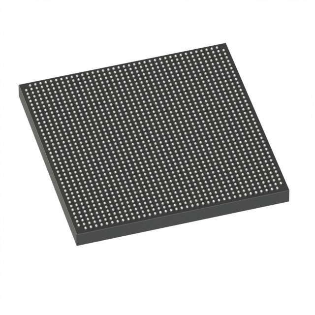
Stratix® V GX Field Programmable Gate Array (FPGA) IC 696 53248000 952000 1517-BBGA, FCBGA |
|---|---|
| Quantity | 655 Available (as of June 15, 2026) |
| Product Category | Field Programmable Gate Array (FPGA) |
|---|---|
| Manufacturer | Intel |
| Manufacturing Status | Active |
| Manufacturer Standard Lead Time | 26 Weeks |
| Datasheet |
Specifications & Environmental
| Device Package | 1517-HBGA (45x45) | Grade | Commercial | Operating Temperature | 0°C – 85°C | ||
|---|---|---|---|---|---|---|---|
| Package / Case | 1517-BBGA, FCBGA | Number of I/O | 696 | Voltage | 870 mV - 930 mV | ||
| Mounting Method | Surface Mount | RoHS Compliance | RoHS Compliant | REACH Compliance | REACH Unaffected | ||
| Moisture Sensitivity Level | 3 (168 Hours) | Number of LABs/CLBs | 359200 | Number of Logic Elements/Cells | 952000 | ||
| Number of Gates | N/A | ECCN | N/A | HTS Code | N/A | ||
| Qualification | N/A | Total RAM Bits | 53248000 |
Overview of 5SGXEABK1H40C2G – Stratix® V GX Field Programmable Gate Array (FPGA), 952,000 logic elements, ~53.25 Mbits RAM, 696 I/O, 1517-BBGA
The 5SGXEABK1H40C2G is a Stratix® V GX series Field Programmable Gate Array (FPGA) optimized for high-density logic and large on‑chip memory requirements. This commercial‑grade FPGA combines a substantial logic fabric with abundant embedded RAM and a high I/O count to support complex, memory‑intensive designs.
Key attributes include 952,000 logic elements, approximately 53.25 Mbits of embedded memory, 696 user I/O, and a 1517‑BBGA FCBGA package. The device operates from 870 mV to 930 mV core supply and is specified for 0 °C to 85 °C operation.
Key Features
- Core Logic 952,000 logic elements provide a large, flexible fabric for implementing complex digital functions and custom hardware accelerators.
- Embedded Memory Approximately 53.25 Mbits of on‑chip RAM to support buffering, tables, and high‑bandwidth local storage without external memory dependencies.
- High I/O Count 696 general‑purpose I/O pins enable extensive board‑level connectivity and broad peripheral interfacing options.
- Power and Voltage Core supply range of 870 mV to 930 mV supports the device’s specified operating conditions for power delivery and planning.
- Package and Mounting 1517‑BBGA (FCBGA) package; supplier device package listed as 1517‑HBGA (45×45). Surface‑mount mounting type for standard PCB assembly flows.
- Temperature and Grade Commercial grade operation over 0 °C to 85 °C for applications targeted at commercial environments.
- Standards Compliance RoHS compliant, supporting regulatory and environmental requirements for lead‑free assemblies.
Typical Applications
- High‑density digital systems Implement large custom logic designs and hardware accelerators using the device’s extensive logic element count and embedded RAM.
- Memory‑intensive processing Use the substantial on‑chip RAM for buffering, lookup tables, and on‑die data handling to reduce external memory bandwidth needs.
- High‑I/O interface designs Leverage 696 I/O pins for dense board connectivity, multiple peripheral interfaces, and complex system integration.
Unique Advantages
- Large programmable fabric: 952,000 logic elements enable consolidation of multi‑module designs onto a single FPGA, reducing BOM and board complexity.
- Substantial on‑chip memory: Approximately 53.25 Mbits of embedded RAM supports local data staging and high‑performance buffering without immediate reliance on off‑chip memory.
- Extensive I/O capacity: 696 I/O pins simplify system partitioning by providing ample signals for peripherals, interfaces, and board‑level routing.
- Commercial temperature suitability: Rated for 0 °C to 85 °C, matching typical commercial systems and controlled ambient environments.
- Surface‑mount BGA packaging: 1517‑BBGA FCBGA package supports high‑density PCB layouts and standard SMT assembly processes.
- Regulatory readiness: RoHS compliance helps meet environmental requirements for modern electronic assemblies.
Why Choose 5SGXEABK1H40C2G?
The 5SGXEABK1H40C2G delivers a combination of high logic density, ample embedded memory, and broad I/O resources in a commercial‑grade Stratix V GX device. Its specification set is suited to engineers and procurement teams designing compact, memory‑heavy digital systems that require substantial on‑chip resources and extensive external interfacing.
This device is a practical choice for designs that demand integration of large logic functions and significant local storage while maintaining standard board assembly and commercial operating temperature requirements. Its inclusion in the Stratix V GX family provides access to ecosystem documentation and device‑level electrical characteristics for detailed system design and validation.
Request a quote or submit an inquiry to evaluate 5SGXEABK1H40C2G for your next high‑density FPGA design project.


Date Founded: 1968
Headquarters: Santa Clara, California, USA
Employees: 130,000+
Revenue: $54.23 Billion
Certifications and Memberships: ISO9001:2015, ISO14001:2015, ISO17025:2017, ISO27001:2022, ISO45001:2018, ISO50001:2018


