
5SGXEA9N3F45I3N
| Part Description |
Stratix® V GX Field Programmable Gate Array (FPGA) IC 840 53248000 840000 1932-BBGA, FCBGA |
|---|---|
| Quantity | 580 Available (as of June 10, 2026) |

| Product Category | Field Programmable Gate Array (FPGA) |
|---|---|
| Manufacturer | Intel |
| Manufacturing Status | Obsolete |
| Manufacturer Standard Lead Time | Contact Us |
| Datasheet |
Specifications & Environmental
| Device Package | 1932-FBGA, FC (45x45) | Grade | Industrial | Operating Temperature | -40°C – 100°C | ||
|---|---|---|---|---|---|---|---|
| Package / Case | 1932-BBGA, FCBGA | Number of I/O | 840 | Voltage | 820 mV - 880 mV | ||
| Mounting Method | Surface Mount | RoHS Compliance | RoHS Compliant | REACH Compliance | REACH Unknown | ||
| Moisture Sensitivity Level | 3 (168 Hours) | Number of LABs/CLBs | 317000 | Number of Logic Elements/Cells | 840000 | ||
| Number of Gates | N/A | ECCN | 3A001A2C | HTS Code | 8542.39.0001 | ||
| Qualification | N/A | Total RAM Bits | 53248000 |
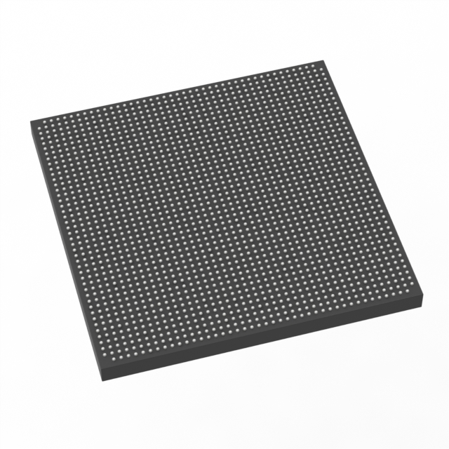
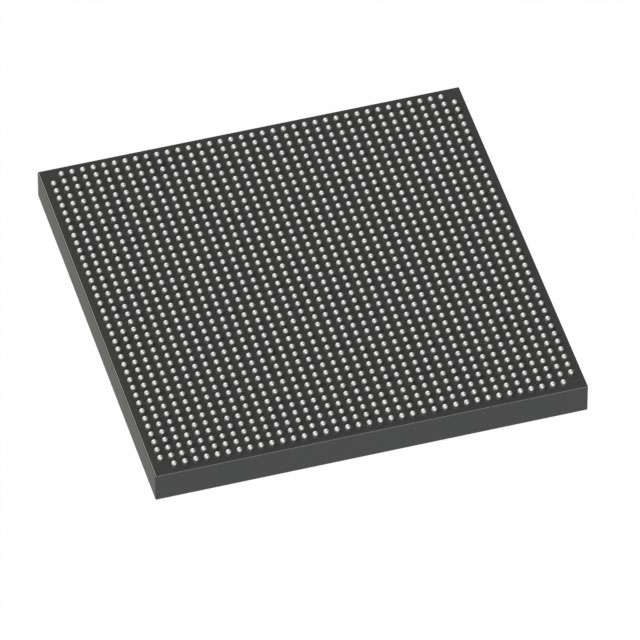
Overview of 5SGXEA9N3F45I3N – Stratix® V GX FPGA IC, 840K logic elements, 1932-BBGA
The 5SGXEA9N3F45I3N is an Intel Stratix® V GX Field Programmable Gate Array (FPGA) provided in a 1932-ball BGA FCBGA package. This industrial-grade device delivers very high logic density and on-chip memory in a surface-mount package designed for complex, high-density FPGA implementations.
With 840,000 logic elements, approximately 53.25 Mbits of embedded RAM and 840 I/O, this device targets applications that require substantial programmable logic, large embedded memory resources, and extensive I/O connectivity while operating across an industrial temperature range.
Key Features
- Logic Capacity Provides 840,000 logic elements for implementing large-scale programmable logic, state machines, and datapath resources.
- Embedded Memory Approximately 53.25 Mbits of on-chip RAM to support buffering, FIFOs, and large on-chip data structures.
- I/O Density 840 I/O pins to support high pin-count interfaces and board-level connectivity.
- Power Supply Core voltage supply range from 820 mV to 880 mV to match Stratix V core power requirements.
- Package & Mounting 1932-BBGA FCBGA package (supplier package: 1932-FBGA, FC (45×45)), delivered in a surface-mount format for compact board integration.
- Operating Range & Grade Industrial-grade device rated for operation from −40 °C to 100 °C for robust performance in demanding environments.
- Standards Compliance RoHS compliant for compatibility with modern manufacturing and environmental requirements.
Typical Applications
- High-density digital systems Use the large logic capacity and embedded RAM for complex datapath implementations, parallel processing, and custom accelerators.
- Networking & communications Leverage high I/O count and family-level transceiver capabilities (Stratix V GX family) for packet processing, switching, and protocol offload tasks.
- Data center and compute acceleration Deploy as a programmable fabric for hardware acceleration, buffering and protocol adaptation where large on-chip memory and logic are required.
Unique Advantages
- High logic density: 840,000 logic elements enable consolidation of multi-function designs into a single FPGA, reducing board-level complexity.
- Substantial on-chip RAM: Approximately 53.25 Mbits of embedded memory supports large buffers and high-throughput streaming without relying on external memory.
- Extensive I/O: 840 I/O pins provide flexibility for multiple interfaces and high channel counts on a single device.
- Industrial operation: Rated for −40 °C to 100 °C, making it suitable for industrial environments requiring wider temperature tolerance.
- Compact, manufacturable package: 1932-ball FCBGA (45×45) surface-mount package offers a high pin count in a compact footprint for dense board-level integration.
- RoHS compliant: Aligns with environmental and manufacturing requirements for modern electronics production.
Why Choose 5SGXEA9N3F45I3N?
The 5SGXEA9N3F45I3N positions itself as a robust, industrial-grade Stratix V GX FPGA option for designs that demand very high logic and memory capacity with broad I/O connectivity. Its combination of 840,000 logic elements, roughly 53.25 Mbits of embedded RAM, and 840 I/O make it well suited to complex, high-density FPGA implementations in networking, compute acceleration, and other performance-focused systems.
Engineers specifying this device benefit from a compact 1932-BBGA surface-mount package and an operating voltage and temperature range aligned with industrial deployments, while maintaining compliance with RoHS requirements for modern production environments.
Request a quote or submit an inquiry to begin procurement or to get detailed availability and lead-time information for this part.


Date Founded: 1968
Headquarters: Santa Clara, California, USA
Employees: 130,000+
Revenue: $54.23 Billion
Certifications and Memberships: ISO9001:2015, ISO14001:2015, ISO17025:2017, ISO27001:2022, ISO45001:2018, ISO50001:2018


