
5SGXEABN2F45C2
| Part Description |
Stratix® V GX Field Programmable Gate Array (FPGA) IC 840 53248000 952000 1932-BBGA, FCBGA |
|---|---|
| Quantity | 1,008 Available (as of June 14, 2026) |

| Product Category | Field Programmable Gate Array (FPGA) |
|---|---|
| Manufacturer | Intel |
| Manufacturing Status | Obsolete |
| Manufacturer Standard Lead Time | Contact Us |
| Datasheet |
Specifications & Environmental
| Device Package | 1932-FBGA, FC (45x45) | Grade | Commercial | Operating Temperature | 0°C – 85°C | ||
|---|---|---|---|---|---|---|---|
| Package / Case | 1932-BBGA, FCBGA | Number of I/O | 840 | Voltage | 870 mV - 930 mV | ||
| Mounting Method | Surface Mount | RoHS Compliance | RoHS non-compliant | REACH Compliance | REACH Unknown | ||
| Moisture Sensitivity Level | 3 (168 Hours) | Number of LABs/CLBs | 359200 | Number of Logic Elements/Cells | 952000 | ||
| Number of Gates | N/A | ECCN | 3A001A7A | HTS Code | 8542.39.0001 | ||
| Qualification | N/A | Total RAM Bits | 53248000 |
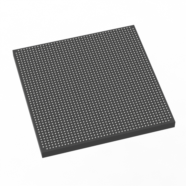
Overview of 5SGXEABN2F45C2 – Stratix® V GX FPGA, 952,000 logic elements, 840 I/O (1932-BBGA)
The 5SGXEABN2F45C2 is an Intel Stratix V GX field-programmable gate array (FPGA) delivered in a 1932-ball FCBGA package for surface-mount applications. Built on a 28-nm process with a high-density core architecture, this GX variant targets high-bandwidth, data-intensive applications that require large logic capacity and extensive I/O.
With 952,000 logic elements, approximately 53.25 Mbits of embedded memory, and support for high-speed transceiver capabilities in the Stratix V GX family, the device is well suited for demanding communications, networking, and packet-processing designs.
Key Features
- Logic Capacity — 952,000 logic elements to support large-scale digital designs and complex system integration.
- Embedded Memory — Approximately 53.25 Mbits of on-chip RAM (53,248,000 bits) provided by M20K embedded memory blocks for buffering, packet storage, and on-chip data handling.
- High I/O Count — 840 I/O pins to enable dense board-level connectivity and broad external interface options.
- Transceiver Capability (Series-Level) — Stratix V GX devices in the family offer up to 66 integrated transceivers with 14.1-Gbps data-rate capability, supporting backplane and optical interface applications.
- Adaptive Logic and DSP Building Blocks — Redesigned adaptive logic modules (ALMs) and variable-precision DSP blocks provide flexible arithmetic and signal-processing resources for compute- and throughput-intensive functions.
- Clocking and Timing — Fractional phase-locked loops (PLLs) and a comprehensive fabric clocking network support complex timing architectures.
- Embedded Hard IP — Includes an Embedded HardCopy Block for hardened IP instantiation such as PCIe Gen1/Gen2/Gen3.
- Process and Core Voltage — Implemented on a 28-nm TSMC process with core voltage options noted in the family (0.85 V or 0.9 V); this specific device lists a supply range of 870 mV to 930 mV.
- Package and Mounting — 1932-ball BBGA (FCBGA) package with surface-mount mounting; supplier package listed as 1932-FBGA, FC (45×45).
- Commercial Temperature Grade — Rated for operation from 0 °C to 85 °C and compliant with RoHS requirements.
Typical Applications
- Optical and Packet Transport — High-bandwidth transport systems such as 40G/100G optical transport and backplane interfaces benefit from large logic resources and high-speed transceiver support.
- Network and Packet Processing — Packet processing, traffic management, and wireline network equipment leverage the device’s logic density, DSP resources, and high I/O count.
- Test and Measurement — Network test equipment and optical test systems use the FPGA’s transceiver capabilities and flexible fabric for protocol emulation and high-speed data capture.
- Communications Systems — Military and commercial communications applications use the device’s combination of logic, memory, and transceivers for high-throughput signal processing and interface tasks.
Unique Advantages
- High Logic Density: 952,000 logic elements accommodate large, integrated designs and reduce the need for multi-chip partitioning.
- Substantial On-Chip Memory: Approximately 53.25 Mbits of embedded memory enables extensive buffering and on-chip data storage, minimizing external memory bandwidth demands.
- Extensive I/O: 840 I/O pins simplify system-level connectivity and support multiple high-speed interfaces without extensive external glue logic.
- Series-Level High-Speed Transceivers: GX-family transceivers (up to 14.1 Gbps, up to 66 channels) provide native support for backplane and optical interfaces.
- Flexible DSP and Clocking Resources: Variable-precision DSP blocks and fractional PLLs give designers deterministic performance for signal processing and timing-critical applications.
- Embedded Hard IP: The Embedded HardCopy Block eases implementation of common protocols such as PCIe Gen1/Gen2/Gen3, reducing integration risk for system IP.
Why Choose 5SGXEABN2F45C2?
The 5SGXEABN2F45C2 delivers a high-density Stratix V GX FPGA implementation that combines large logic capacity, extensive on-chip memory, and a high I/O count in a 1932-ball FCBGA package. Its architecture and family-level transceiver capabilities make it suitable for designs that require substantial bandwidth and complex signal-processing resources.
This device is targeted at engineers and system architects building communications, networking, and test equipment where integration density, on-chip memory, and connectivity are primary concerns. Backed by the Stratix V device family features, it offers a scalable platform supported by comprehensive device-level building blocks and hardened IP options.
Request a quote or submit a sales inquiry to evaluate availability, pricing, and lead times for the 5SGXEABN2F45C2.


Date Founded: 1968
Headquarters: Santa Clara, California, USA
Employees: 130,000+
Revenue: $54.23 Billion
Certifications and Memberships: ISO9001:2015, ISO14001:2015, ISO17025:2017, ISO27001:2022, ISO45001:2018, ISO50001:2018


