
5SGXEB6R2F40C1G
| Part Description |
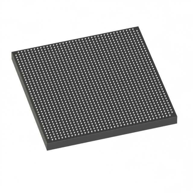
Stratix® V GX Field Programmable Gate Array (FPGA) IC 432 53248000 597000 1517-FBGA (40x40) |
|---|---|
| Quantity | 652 Available (as of June 14, 2026) |

| Product Category | Field Programmable Gate Array (FPGA) |
|---|---|
| Manufacturer | Intel |
| Manufacturing Status | Active |
| Manufacturer Standard Lead Time | 26 Weeks |
| Datasheet |
Specifications & Environmental
| Device Package | 1517-FBGA (40x40) | Grade | Commercial | Operating Temperature | 0°C – 85°C | ||
|---|---|---|---|---|---|---|---|
| Package / Case | 1517-FBGA (40x40) | Number of I/O | 432 | Voltage | 870 mV - 930 mV | ||
| Mounting Method | Surface Mount | RoHS Compliance | RoHS Compliant | REACH Compliance | REACH Unaffected | ||
| Moisture Sensitivity Level | 3 (168 Hours) | Number of LABs/CLBs | 225400 | Number of Logic Elements/Cells | 597000 | ||
| Number of Gates | N/A | ECCN | N/A | HTS Code | N/A | ||
| Qualification | N/A | Total RAM Bits | 53248000 |
Overview of 5SGXEB6R2F40C1G – Stratix® V GX FPGA, 597,000 logic elements, 432 I/O, 1517-FBGA
The 5SGXEB6R2F40C1G is a Stratix® V GX Field Programmable Gate Array (FPGA) IC delivering very high logic density, substantial embedded memory, and extensive I/O in a compact ball-grid array package. It is a commercial-grade Stratix V GX device intended for designs that require large on-chip resources and significant I/O connectivity.
With 597,000 logic elements and approximately 53.25 Mbits of embedded RAM, this device targets high‑capacity digital implementations where integration and I/O count are primary drivers. The device operates within a 0 °C to 85 °C commercial temperature range and uses an 1517‑FBGA (40×40) surface‑mount package.
Key Features
- Core / Logic: 597,000 logic elements provide a high logic density for complex FPGA designs. The product data also indicates 225,400 logic array blocks for resource breakdown and planning.
- Embedded Memory: Approximately 53.25 Mbits of on‑chip RAM for large buffering, state storage, and memory‑intensive logic functions.
- I/O Capacity: 432 I/O pins to support multiple interfaces, parallel buses, or extensive external connectivity.
- Power Supply: Core voltage range specified at 870 mV to 930 mV to match system power delivery requirements.
- Package & Mounting: 1517‑FBGA (40×40) supplier device package with surface mount mounting for compact board integration.
- Temperature & Grade: Commercial temperature grade with an operating range of 0 °C to 85 °C.
- Regulatory: RoHS compliant.
- Series Transceiver Capability (series data): Stratix V GX devices in the series include defined transceiver speed grades (series documentation lists GX channel grades up to 14.1 Gbps).
Typical Applications
- High‑density digital systems: Implement complex state machines, wide datapaths, and large custom logic functions using the device’s large logic and memory resources.
- High‑I/O interfaces: Use the 432 I/O pins for multi‑lane interfaces, parallel buses, or multi‑peripheral connectivity where board routing and pin count are critical.
- Prototyping and hardware acceleration: Leverage the logic capacity and embedded RAM for FPGA‑based prototyping, algorithm acceleration, and emulation tasks.
- Compact board designs: The 1517‑FBGA (40×40) surface‑mount package supports high resource density in constrained PCB areas.
Unique Advantages
- High logic capacity: 597,000 logic elements enable implementation of large, integrated designs without partitioning across multiple devices.
- Generous embedded memory: Approximately 53.25 Mbits of on‑chip RAM reduces dependence on external memory for intermediate storage and buffering.
- Extensive I/O: 432 I/O pins simplify board‑level interfacing and reduce the need for additional interface ICs.
- Commercial temperature suitability: Rated for 0 °C to 85 °C, matching typical commercial and lab environments.
- Compact package: The 1517‑FBGA (40×40) package provides a balance of high resource density and manageable board footprint.
- Environmental compliance: RoHS compliance supports regulatory and environmental requirements.
Why Choose 5SGXEB6R2F40C1G?
The 5SGXEB6R2F40C1G positions itself as a high‑capacity commercial Stratix V GX FPGA well suited to designs that need substantial on‑chip logic, memory, and I/O within a compact FBGA package. Its combination of 597,000 logic elements, approximately 53.25 Mbits of embedded RAM, and 432 I/O make it appropriate for advanced digital systems, prototyping, and applications where integration and pin count are key considerations.
Selecting this device supports designs that require scalability of logic resources and on‑chip memory while maintaining RoHS compliance and standard commercial temperature operation. The device’s specified core voltage range and package format allow straightforward integration into existing power and PCB architectures.
Request a quote or submit an inquiry for pricing and availability for the 5SGXEB6R2F40C1G Stratix® V GX FPGA.


Date Founded: 1968
Headquarters: Santa Clara, California, USA
Employees: 130,000+
Revenue: $54.23 Billion
Certifications and Memberships: ISO9001:2015, ISO14001:2015, ISO17025:2017, ISO27001:2022, ISO45001:2018, ISO50001:2018


