
5SGXEB6R1F43C2LN
| Part Description |
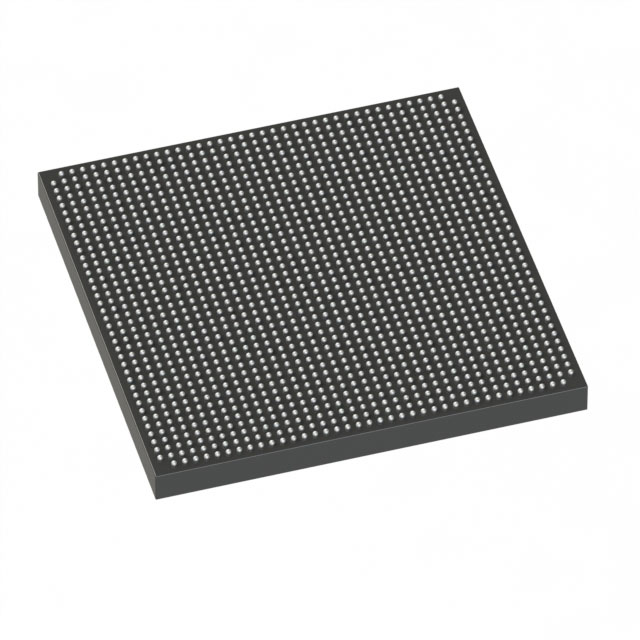
Stratix® V GX Field Programmable Gate Array (FPGA) IC 600 53248000 597000 1760-BBGA, FCBGA |
|---|---|
| Quantity | 280 Available (as of June 15, 2026) |

| Product Category | Field Programmable Gate Array (FPGA) |
|---|---|
| Manufacturer | Intel |
| Manufacturing Status | Obsolete |
| Manufacturer Standard Lead Time | Contact Us |
| Datasheet |
Specifications & Environmental
| Device Package | 1760-FCBGA (42.5x42.5) | Grade | Commercial | Operating Temperature | 0°C – 85°C | ||
|---|---|---|---|---|---|---|---|
| Package / Case | 1760-BBGA, FCBGA | Number of I/O | 600 | Voltage | 820 mV - 880 mV | ||
| Mounting Method | Surface Mount | RoHS Compliance | RoHS Compliant | REACH Compliance | REACH Unknown | ||
| Moisture Sensitivity Level | 3 (168 Hours) | Number of LABs/CLBs | 225400 | Number of Logic Elements/Cells | 597000 | ||
| Number of Gates | N/A | ECCN | 3A001A2C | HTS Code | 8542.39.0001 | ||
| Qualification | N/A | Total RAM Bits | 53248000 |
Overview of 5SGXEB6R1F43C2LN – Stratix® V GX Field Programmable Gate Array (FPGA), 597,000 logic elements, 600 I/O, 1760-FCBGA
The 5SGXEB6R1F43C2LN is a Stratix® V GX family FPGA IC from Intel, delivering high on-chip logic capacity and substantial embedded memory in a high-pin-count FCBGA package. It is intended for commercial-temperature systems that require dense logic arrays, large on-chip RAM, and extensive I/O connectivity.
With approximately 597,000 logic elements, roughly 53.25 Mbits of embedded memory, and up to 600 I/O pins, this device targets designs that integrate complex digital logic, large buffers or scratch memory, and numerous board-level interfaces while operating from a core supply in the 820 mV–880 mV range.
Key Features
- Core Logic Capacity Approximately 597,000 logic elements to support large, integrated digital designs and complex system functions.
- Embedded Memory Approximately 53.25 Mbits of on-chip RAM for buffering, FIFOs, and memory-intensive algorithms without relying on external memory for many tasks.
- High I/O Count Up to 600 I/O pins to support dense board-level interfacing and multi-channel connectivity.
- Package 1760-ball FCBGA (1760-FCBGA, 42.5 × 42.5 mm) surface-mount package for compact board integration with a high pin density.
- Power Supply Core voltage supply range of 820 mV to 880 mV to match platform power-rail requirements.
- Operating Grade and Temperature Commercial grade specified for operation from 0 °C to 85 °C.
- Regulatory RoHS compliant.
Typical Applications
- High‑density logic integration Use the large logic element count to consolidate multiple functions into a single device and simplify board-level design.
- Memory‑intensive buffering Embedded RAM capacity supports on-chip buffering, packet queues, and intermediate data storage for streaming or packetized data flows.
- High‑pin-count interface systems The 600 I/O pins enable multiple parallel interfaces, sensor arrays, or multi-channel data acquisition front ends.
- Complex system prototyping Provides on-chip resources suitable for prototyping integrated systems that require significant logic and memory in a single FPGA.
Unique Advantages
- High logic density: Approximately 597,000 logic elements reduce the need for multiple FPGAs in large designs, simplifying BOM and board layout.
- Substantial on‑chip memory: Approximately 53.25 Mbits of embedded RAM enables larger data buffers and reduces dependency on external memory for many use cases.
- Extensive I/O availability: 600 I/O pins provide flexibility for complex interfacing and parallel channel implementations.
- Space-efficient FCBGA packaging: 1760-FCBGA (42.5 × 42.5 mm) delivers high pin count in a compact footprint for dense board designs.
- Commercial temperature rating: Qualified for 0 °C to 85 °C operation, matching many commercial and enterprise system requirements.
- RoHS compliant: Meets common environmental compliance requirements for electronics manufacturing.
Why Choose 5SGXEB6R1F43C2LN?
The 5SGXEB6R1F43C2LN positions itself as a high-capacity Stratix V GX FPGA option for designers who need significant on-chip logic and memory combined with a large number of I/Os in a single device. Its commercial temperature grade, tight core voltage window, and FCBGA packaging make it suitable for dense, performance-oriented board designs where integration and reduced external components are priorities.
Choose this device for projects that require consolidated digital functions, substantial embedded buffering, and flexible interface options while maintaining a compact board footprint and RoHS compliance.
Request a quote or submit an inquiry to obtain pricing and availability for 5SGXEB6R1F43C2LN and to discuss how this Stratix V GX FPGA can fit your next design.


Date Founded: 1968
Headquarters: Santa Clara, California, USA
Employees: 130,000+
Revenue: $54.23 Billion
Certifications and Memberships: ISO9001:2015, ISO14001:2015, ISO17025:2017, ISO27001:2022, ISO45001:2018, ISO50001:2018


