
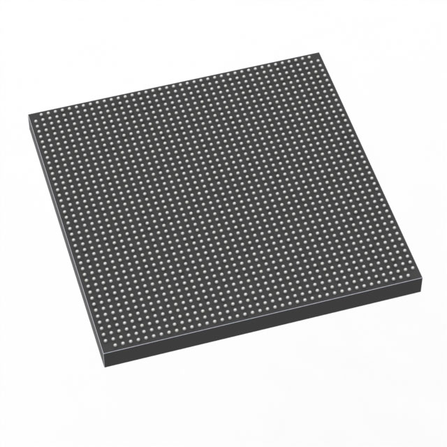
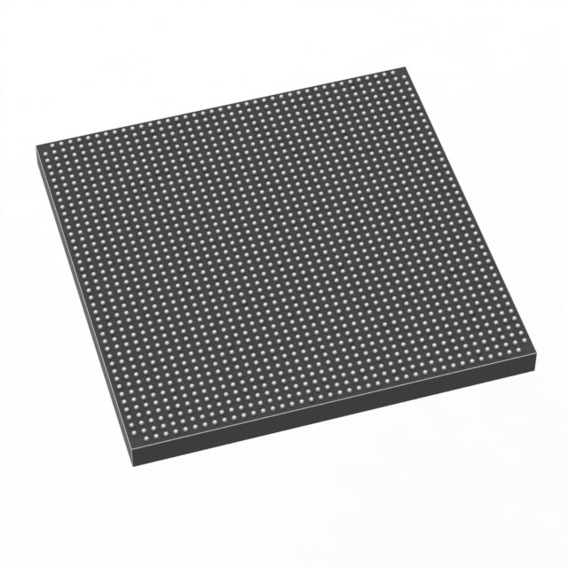
5SGXEB6R1F43C2G
| Part Description |
Stratix® V GX Field Programmable Gate Array (FPGA) IC 600 53248000 597000 1760-BBGA, FCBGA |
|---|---|
| Quantity | 1,175 Available (as of October 8, 2026) |
| Product Category | Field Programmable Gate Array (FPGA) |
|---|---|
| Manufacturer | Intel |
| Manufacturing Status | Active |
| Manufacturer Standard Lead Time | 26 Weeks |
| Datasheet |
Specifications & Environmental
| Device Package | 1760-FCBGA (42.5x42.5) | Grade | Commercial | Operating Temperature | 0°C – 85°C | ||
|---|---|---|---|---|---|---|---|
| Package / Case | 1760-BBGA, FCBGA | Number of I/O | 600 | Voltage | 870 mV - 930 mV | ||
| Mounting Method | Surface Mount | RoHS Compliance | RoHS Compliant | REACH Compliance | REACH Unaffected | ||
| Moisture Sensitivity Level | 3 (168 Hours) | Number of LABs/CLBs | 225400 | Number of Logic Elements/Cells | 597000 | ||
| Number of Gates | N/A | ECCN | N/A | HTS Code | N/A | ||
| Qualification | N/A | Total RAM Bits | 53248000 |
Overview of 5SGXEB6R1F43C2G – Stratix® V GX FPGA, 1760‑FCBGA
The 5SGXEB6R1F43C2G is a Stratix V GX field‑programmable gate array (FPGA) in a 1760‑FBGA FCBGA package, offered in a commercial temperature grade. It delivers a very large logic fabric and on‑chip memory, plus a high I/O count for complex, high‑integration designs.
As part of the Stratix V GX family, the device targets applications that require large logic capacity, substantial embedded RAM, and extensive I/O connectivity. The Stratix V GX series datasheet documents multiple transceiver speed grades for the family, including GX channel options up to 14.1 Gbps in certain speed grades.
Key Features
- Logic Capacity — 597,000 logic elements (logic cells) to implement large, multi‑domain designs and complex algorithms.
- Embedded Memory — Approximately 53.25 Mbits of on‑chip RAM to support large buffers, FIFOs, and lookup tables without external memory.
- I/O Resources — 600 user I/Os to connect to wide parallel buses, high‑pin count peripherals, and multi‑lane interfaces.
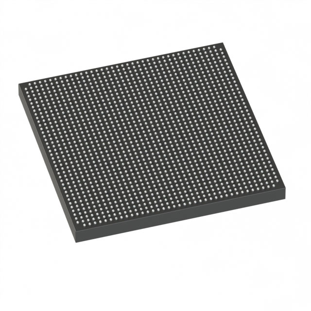
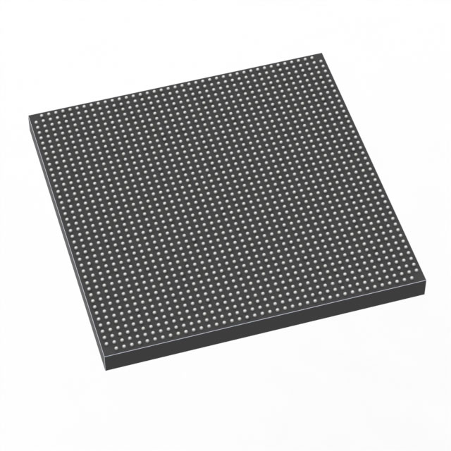
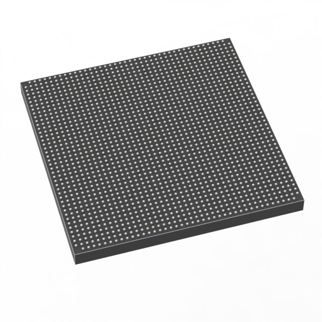
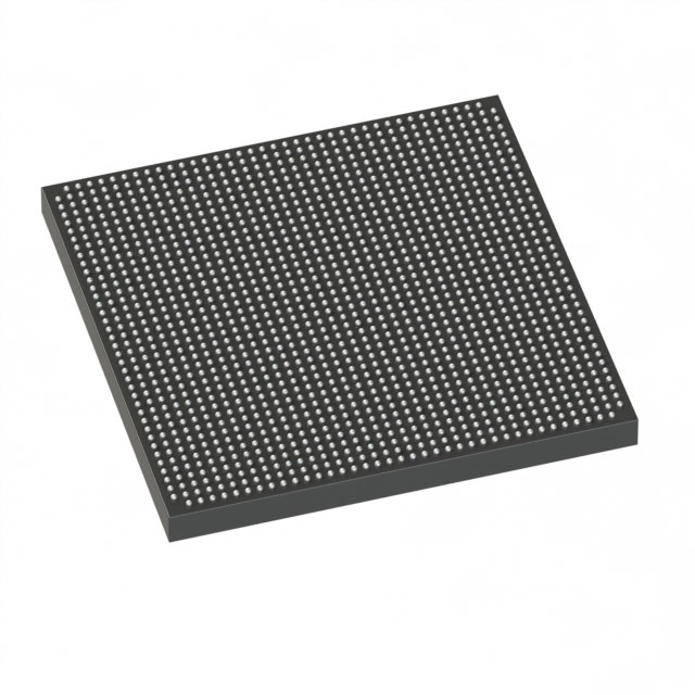
- Package — 1760‑FBGA (1760‑FCBGA) surface‑mount package; supplier device package specified as 1760‑FCBGA (42.5 × 42.5 mm).
- Power / Core Supply — Core supply range from 870 mV to 930 mV, enabling compatibility with targeted core power rails.
- Temperature & Grade — Commercial grade operation from 0 °C to 85 °C for typical commercial environments.
- Compliance — RoHS compliant.
- Series Transceiver Options — The Stratix V GX family includes transceiver speed grades documented up to 14.1 Gbps (family‑level specification).
Typical Applications
- High‑density FPGA compute — Large logic and memory resources are suitable for hardware acceleration, signal processing blocks, and complex state machines.
- High‑pin I/O systems — 600 I/Os enable wide parallel interfaces, multi‑lane video, or custom board‑level connectivity.
- Memory‑intensive buffering — Approximately 53.25 Mbits of embedded RAM supports large on‑chip FIFOs, frame buffers, and packet buffering.
- Multi‑function system integration — The combination of logic, RAM, and I/O helps consolidate multiple discrete functions into a single FPGA‑based subsystem.
Unique Advantages
- High logic density: 597,000 logic elements allow implementation of large, partitioned designs without excessive external logic.
- Substantial on‑chip memory: Approximately 53.25 Mbits of RAM reduces dependence on external memory for buffering and local data storage.
- Extensive I/O availability: 600 I/Os support broad peripheral and bus connectivity, simplifying board‑level routing for complex systems.
- Compact high‑pin package: 1760‑FCBGA (42.5 × 42.5 mm) provides the pin count needed for dense designs in a defined footprint.
- Commercial temperature grading: Specified operation from 0 °C to 85 °C for mainstream commercial deployments.
- RoHS compliant: Meets environmental compliance expectations for commercial electronic products.
Why Choose 5SGXEB6R1F43C2G?
The 5SGXEB6R1F43C2G positions itself as a high‑capacity, commercially graded Stratix V GX FPGA suitable for engineers who need large logic and embedded memory with a high I/O count in a compact FCBGA package. Its documented family transceiver options and substantial on‑chip resources make it well suited for complex data flow, buffering, and integration tasks on commercial designs.
Choose this device when your design requires significant on‑chip resources and I/O connectivity combined with the ecosystem and documentation of the Stratix V family. The device’s package, voltage range, temperature rating, and RoHS compliance provide clear, verifiable characteristics to support procurement and system design decisions.
Request a quote or submit an inquiry to receive pricing, availability, and further ordering information for 5SGXEB6R1F43C2G.





















Date Founded: 1968
Headquarters: Santa Clara, California, USA
Employees: 130,000+
Revenue: $54.23 Billion
Certifications and Memberships: ISO9001:2015, ISO14001:2015, ISO17025:2017, ISO27001:2022, ISO45001:2018, ISO50001:2018


