
5SGXEB9R2H43C2LG
| Part Description |
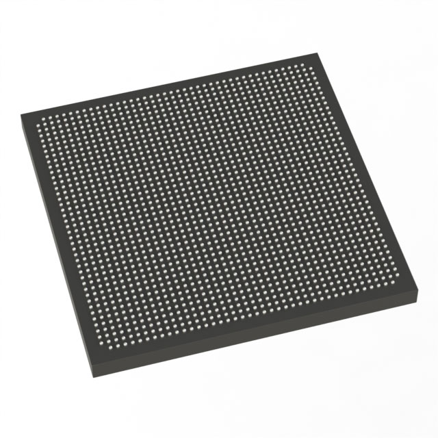
Stratix® V GX Field Programmable Gate Array (FPGA) IC 600 53248000 840000 1760-BBGA, FCBGA |
|---|---|
| Quantity | 1,331 Available (as of June 15, 2026) |

| Product Category | Field Programmable Gate Array (FPGA) |
|---|---|
| Manufacturer | Intel |
| Manufacturing Status | Active |
| Manufacturer Standard Lead Time | 26 Weeks |
| Datasheet |
Specifications & Environmental
| Device Package | 1760-HBGA (45x45) | Grade | Commercial | Operating Temperature | 0°C – 85°C | ||
|---|---|---|---|---|---|---|---|
| Package / Case | 1760-BBGA, FCBGA | Number of I/O | 600 | Voltage | 820 mV - 880 mV | ||
| Mounting Method | Surface Mount | RoHS Compliance | RoHS Compliant | REACH Compliance | REACH Unaffected | ||
| Moisture Sensitivity Level | 3 (168 Hours) | Number of LABs/CLBs | 317000 | Number of Logic Elements/Cells | 840000 | ||
| Number of Gates | N/A | ECCN | N/A | HTS Code | N/A | ||
| Qualification | N/A | Total RAM Bits | 53248000 |
Overview of 5SGXEB9R2H43C2LG – Stratix® V GX Field Programmable Gate Array (FPGA), 840,000 logic elements
The 5SGXEB9R2H43C2LG is a Stratix® V GX FPGA IC from Intel, delivering very large programmable logic capacity and extensive I/O for complex system designs. Built for high-density, programmable logic applications, it pairs 840,000 logic elements with approximately 53 Mbits of embedded memory and up to 600 I/Os to support demanding on-board processing and interface integration.
This device is supplied in a 1760-BBGA (FCBGA) package with a 1760-HBGA (45×45) supplier package variant, operates with a core supply range of 820 mV to 880 mV, and is graded for commercial temperature operation from 0 °C to 85 °C. It is RoHS compliant and designed for surface-mount PCB assembly.
Key Features
- Core Logic Capacity 840,000 logic elements for large-scale, highly parallel programmable logic implementations.
- Embedded Memory Approximately 53 Mbits of on-chip RAM to support buffering, LUTs, and data-path storage without external memory.
- I/O Resources Up to 600 I/O pins to enable dense connectivity to peripherals, memories, and high-speed interfaces.
- Power Supply Core voltage supply range of 820 mV to 880 mV to match system power-rail design requirements.
- Package & Mounting Delivered in a 1760-BBGA (FCBGA) package; supplier device package listed as 1760-HBGA (45×45). Surface-mount mounting type for standard PCB assembly.
- Operating Temperature Commercial-grade operation from 0 °C to 85 °C for typical commercial and enterprise applications.
- Compliance RoHS compliant for lead-free manufacturing and regulatory alignment.
Typical Applications
- High-density FPGA designs Implement large custom logic networks and complex state machines using the device's 840,000 logic elements and abundant embedded memory.
- Data-path acceleration On-chip memory and extensive I/O enable buffering and parallel processing for packet handling, signal processing, and hardware acceleration tasks.
- Prototyping and system integration Use the device as a platform for integrating multiple functions and interfaces on a single FPGA for board-level prototyping and system consolidation.
Unique Advantages
- Large programmable fabric: 840,000 logic elements reduce the need for multiple FPGAs in high-density designs, simplifying system architecture.
- Significant on-chip memory: Approximately 53 Mbits of embedded RAM supports deep buffering and local data storage to improve throughput and reduce external memory bandwidth requirements.
- Extensive I/O availability: Up to 600 I/Os provide flexible connectivity options for multi-channel interfaces and peripheral integration.
- Compact, surface-mount package: The 1760-BBGA/1760-HBGA package enables high pin-count in a controlled PCB footprint for dense board layouts.
- Commercial temperature rating: Operates from 0 °C to 85 °C to meet typical commercial and enterprise deployment environments.
- RoHS compliance: Supports lead-free manufacturing requirements for modern electronics supply chains.
Why Choose 5SGXEB9R2H43C2LG?
The 5SGXEB9R2H43C2LG offers a combination of very large logic capacity, substantial embedded memory, and extensive I/O in a high-pin-count BGA package—making it suitable for dense, integrated FPGA designs where consolidation and on-chip resources matter. Its commercial-grade temperature rating and RoHS compliance align with mainstream production and regulatory needs.
This device is targeted at designs that require substantial programmable logic and memory resources on a single FPGA, such as compute acceleration, complex protocol handling, and multifunction system prototypes. Designers can rely on the detailed electrical and switching characteristics provided in the Stratix V documentation when validating power and timing for their systems.
Request a quote or submit a product inquiry to receive pricing, availability, and support information for 5SGXEB9R2H43C2LG.


Date Founded: 1968
Headquarters: Santa Clara, California, USA
Employees: 130,000+
Revenue: $54.23 Billion
Certifications and Memberships: ISO9001:2015, ISO14001:2015, ISO17025:2017, ISO27001:2022, ISO45001:2018, ISO50001:2018


