
5SGXEB9R2H43C2LN
| Part Description |
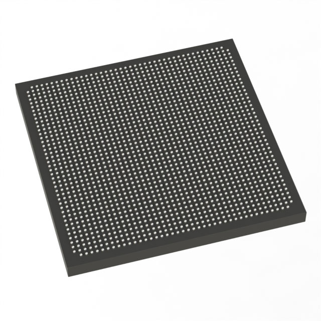
Stratix® V GX Field Programmable Gate Array (FPGA) IC 600 53248000 840000 1760-BBGA, FCBGA |
|---|---|
| Quantity | 1,209 Available (as of June 15, 2026) |

| Product Category | Field Programmable Gate Array (FPGA) |
|---|---|
| Manufacturer | Intel |
| Manufacturing Status | Obsolete |
| Manufacturer Standard Lead Time | Contact Us |
| Datasheet |
Specifications & Environmental
| Device Package | 1760-HBGA (45x45) | Grade | Commercial | Operating Temperature | 0°C – 85°C | ||
|---|---|---|---|---|---|---|---|
| Package / Case | 1760-BBGA, FCBGA | Number of I/O | 600 | Voltage | 820 mV - 880 mV | ||
| Mounting Method | Surface Mount | RoHS Compliance | RoHS Compliant | REACH Compliance | REACH Unknown | ||
| Moisture Sensitivity Level | 3 (168 Hours) | Number of LABs/CLBs | 317000 | Number of Logic Elements/Cells | 840000 | ||
| Number of Gates | N/A | ECCN | 3A001A2C | HTS Code | 8542.39.0001 | ||
| Qualification | N/A | Total RAM Bits | 53248000 |
Overview of 5SGXEB9R2H43C2LN – Stratix V GX FPGA, 840,000 Logic Elements, ~53.248 Mbits RAM, 600 I/Os
The 5SGXEB9R2H43C2LN is an Intel Stratix® V GX field-programmable gate array (FPGA) in a 1760-BBGA FCBGA package. It delivers high logic density and on-chip memory with a large I/O count, packaged for surface-mount PCB assembly and specified for commercial temperature operation.
Designed for applications that require substantial programmable logic, embedded memory and extensive I/O, this device provides integration and capacity tied directly to its electrical and packaging specifications, including a nominal supply range of 820 mV to 880 mV and an operating temperature range of 0 °C to 85 °C.
Key Features
- Core Logic Approximately 840,000 logic elements for implementing large-scale digital designs.
- Embedded Memory Approximately 53.248 Mbits of on-chip RAM for buffering, state storage and large internal data structures.
- I/O Density 600 user I/Os to support wide parallel interfaces and extensive external connectivity.
- Device Capacity Device contains roughly 317,000 LABs/CLBs equivalent (reported as 317000 in product data) to organize logic resources efficiently.
- Power Supply Core supply range specified from 820 mV to 880 mV to meet the device’s operating requirements.
- Package & Mounting 1760-BBGA (FCBGA) package, supplier package 1760-HBGA (45×45), surface-mount mounting for high-density PCB designs.
- Temperature & Grade Commercial grade device rated for operation from 0 °C to 85 °C.
- Environmental Compliance RoHS compliant to support environmental and manufacturing requirements.
Typical Applications
- Large-scale programmable logic Implement complex custom logic functions and state machines using approximately 840,000 logic elements and the device’s LAB/CLB capacity.
- On-chip buffering and data storage Use approximately 53.248 Mbits of embedded RAM for packet buffering, frame storage or large internal FIFOs.
- High-pin-count interfacing Leverage 600 I/Os for broad parallel bus interfaces, front-end connectivity, or extensive sensor and peripheral attachments.
Unique Advantages
- High integration density: The combination of ~840k logic elements and ~53.248 Mbits of embedded memory reduces external component count and simplifies board-level architecture.
- Broad I/O capability: 600 I/Os enable flexible, high-channel-count connectivity without immediate reliance on external multiplexing.
- Compact, manufacturable package: 1760-BBGA (FCBGA) surface-mount package supports high-density PCB designs while providing a standardized 45×45 supplier package footprint.
- Defined commercial operating range: Specified 0 °C to 85 °C operation and commercial grade classification simplify selection for commercial product deployments.
- Controlled core supply: Narrow core voltage range (820 mV–880 mV) supports predictable power design and system-level power budgeting.
- RoHS compliance: Meets environmental directives for lead-free manufacturing and global supply chain requirements.
Why Choose 5SGXEB9R2H43C2LN?
The 5SGXEB9R2H43C2LN offers a large programmable fabric and substantial embedded memory in a single, surface-mount FCBGA package, making it suitable for designs that require extensive on-chip resources and high I/O counts within a commercial temperature envelope. Its clear electrical and packaging specifications support predictable system integration and power planning.
This part is appropriate for engineering teams and procurement organizations seeking a high-density Stratix V GX device with verified on-chip resources and RoHS compliance. The device’s capacity and package choices provide a solid foundation for scalable, high-capacity FPGA implementations backed by Intel’s Stratix V device family documentation.
Request a quote or submit a product inquiry to receive pricing and availability details for the 5SGXEB9R2H43C2LN.


Date Founded: 1968
Headquarters: Santa Clara, California, USA
Employees: 130,000+
Revenue: $54.23 Billion
Certifications and Memberships: ISO9001:2015, ISO14001:2015, ISO17025:2017, ISO27001:2022, ISO45001:2018, ISO50001:2018


