
5SGXMA3K2F35C1G
| Part Description |
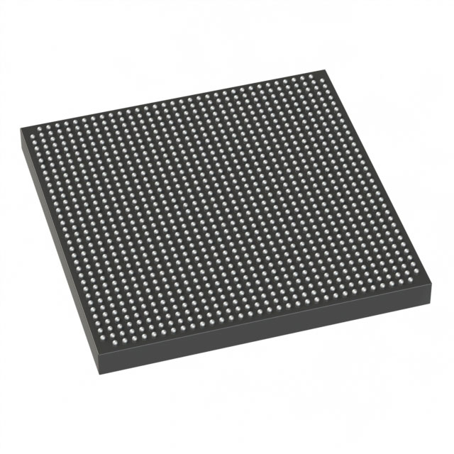
Stratix® V GX Field Programmable Gate Array (FPGA) IC 600 19456000 340000 1152-BBGA, FCBGA |
|---|---|
| Quantity | 1,854 Available (as of June 17, 2026) |
| Product Category | Field Programmable Gate Array (FPGA) |
|---|---|
| Manufacturer | Intel |
| Manufacturing Status | Active |
| Manufacturer Standard Lead Time | 26 Weeks |
| Datasheet |
Specifications & Environmental
| Device Package | 1152-FBGA (35x35) | Grade | Commercial | Operating Temperature | 0°C – 85°C | ||
|---|---|---|---|---|---|---|---|
| Package / Case | 1152-BBGA, FCBGA | Number of I/O | 600 | Voltage | 870 mV - 930 mV | ||
| Mounting Method | Surface Mount | RoHS Compliance | RoHS Compliant | REACH Compliance | REACH Unaffected | ||
| Moisture Sensitivity Level | 3 (168 Hours) | Number of LABs/CLBs | 128300 | Number of Logic Elements/Cells | 340000 | ||
| Number of Gates | N/A | ECCN | N/A | HTS Code | N/A | ||
| Qualification | N/A | Total RAM Bits | 19456000 |
Overview of 5SGXMA3K2F35C1G – Stratix® V GX Field Programmable Gate Array (FPGA) IC, 1152‑BBGA
The 5SGXMA3K2F35C1G is a Stratix V GX Field Programmable Gate Array (FPGA) from Intel, supplied in a 1152‑BBGA (1152‑FBGA, 35×35) surface‑mount package. This commercial‑grade device is built for high‑capacity, board‑level digital logic and I/O integration where large logic resources, substantial on‑chip memory, and a high I/O count are required.
With a large logic fabric and significant embedded RAM, the device is suitable for designs that demand extensive custom logic, complex data buffering, and dense external interfacing while operating within a low core voltage range.
Key Features
- Core Logic Capacity — Provides 340,000 logic elements for implementing sizable custom logic, signal processing, and control functions.
- Embedded Memory — Approximately 19.456 Mbits of on‑chip RAM to support data buffering, FIFOs, and local storage without external memory for many use cases.
- High I/O Count — 600 I/O pins to enable rich peripheral connectivity, parallel interfaces, and large I/O buses.
- Package & Mounting — 1152‑BBGA / 1152‑FBGA (35×35) footprint, surface mount mounting type for compact, high‑density board designs.
- Power Supply — Core voltage supply range of 870 mV to 930 mV, supporting low‑voltage core operation.
- Operating Conditions — Commercial temperature grade with an operating range of 0 °C to 85 °C.
- Compliance — RoHS compliant.
Typical Applications
- High‑density logic and signal processing — Use the large logic element count and embedded RAM for FPGA‑based algorithms, custom accelerators, and protocol processing.
- High‑pin peripheral systems — The 600 I/Os support wide parallel interfaces, multiple GPIO banks, and complex board interconnects.
- Communications and data handling — Stratix V GX family characteristics and device resources suit designs that require substantial on‑chip buffering and dense I/O for networking and data aggregation.
Unique Advantages
- Extensive logic resources: 340,000 logic elements enable large, integrated designs that reduce the need for multiple devices.
- Significant embedded memory: Approximately 19.456 Mbits of on‑chip RAM minimizes external memory dependency for many buffering and scratchpad requirements.
- High connectivity: 600 available I/Os allow flexible interfacing to peripherals, sensors, and high‑bandwidth buses.
- Compact BGA package: 1152‑FBGA (35×35) provides a high pin density in a board‑efficient form factor suitable for space‑constrained systems.
- Low core voltage: Operates in a narrow core voltage window (870 mV–930 mV), consistent with modern low‑power FPGA architectures.
- RoHS compliant: Conforms to lead‑free manufacturing requirements for environmentally regulated designs.
Why Choose 5SGXMA3K2F35C1G?
The 5SGXMA3K2F35C1G positions itself as a high‑capacity, commercially graded Stratix V GX FPGA optimized for designs that need a combination of large programmable logic, ample embedded RAM, and a high I/O count in a compact BGA package. Its specifications make it suitable for developers and system integrators building complex digital processing, high‑connectivity controllers, and data handling applications.
Choosing this FPGA provides design scalability and integration potential through abundant logic and memory resources, a dense pinout for extensive interfacing, and compliance with RoHS requirements—supporting both prototype and production deployments within its specified operating range.
Request a quote or submit an inquiry for pricing and availability to evaluate the 5SGXMA3K2F35C1G for your next design.


Date Founded: 1968
Headquarters: Santa Clara, California, USA
Employees: 130,000+
Revenue: $54.23 Billion
Certifications and Memberships: ISO9001:2015, ISO14001:2015, ISO17025:2017, ISO27001:2022, ISO45001:2018, ISO50001:2018


