
5SGXMA4K1F40C2G
| Part Description |
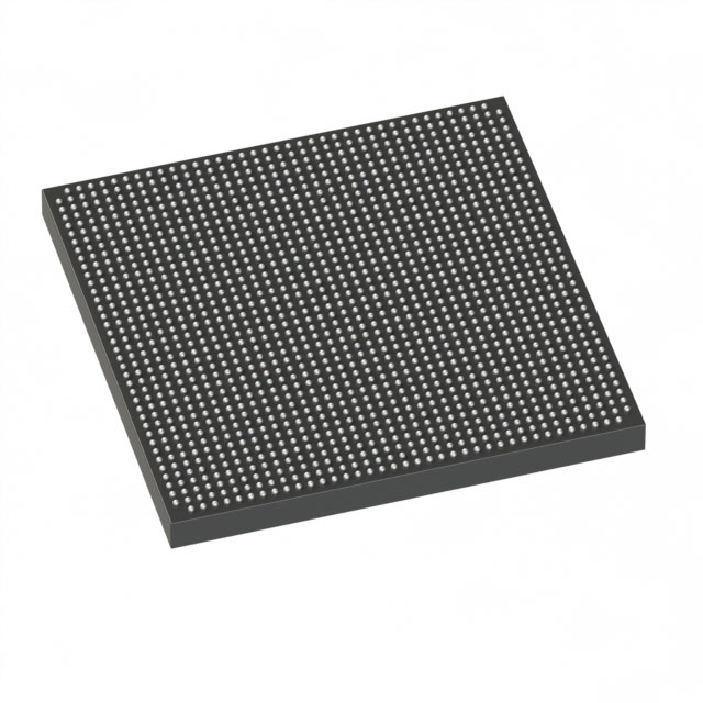
Stratix® V GX Field Programmable Gate Array (FPGA) IC 600 37888000 420000 1517-BBGA, FCBGA |
|---|---|
| Quantity | 535 Available (as of June 14, 2026) |

| Product Category | Field Programmable Gate Array (FPGA) |
|---|---|
| Manufacturer | Intel |
| Manufacturing Status | Active |
| Manufacturer Standard Lead Time | 26 Weeks |
| Datasheet |
Specifications & Environmental
| Device Package | 1517-FBGA (40x40) | Grade | Commercial | Operating Temperature | 0°C – 85°C | ||
|---|---|---|---|---|---|---|---|
| Package / Case | 1517-BBGA, FCBGA | Number of I/O | 600 | Voltage | 870 mV - 930 mV | ||
| Mounting Method | Surface Mount | RoHS Compliance | RoHS Compliant | REACH Compliance | REACH Unaffected | ||
| Moisture Sensitivity Level | 3 (168 Hours) | Number of LABs/CLBs | 158500 | Number of Logic Elements/Cells | 420000 | ||
| Number of Gates | N/A | ECCN | N/A | HTS Code | N/A | ||
| Qualification | N/A | Total RAM Bits | 37888000 |
Overview of 5SGXMA4K1F40C2G – Stratix® V GX FPGA — 420,000 logic elements, 600 I/Os
The 5SGXMA4K1F40C2G is a Stratix V GX Field Programmable Gate Array (FPGA) IC from Intel. It delivers a high-density programmable fabric with extensive on-chip memory and a large I/O count, intended for advanced digital designs within commercial temperature environments.
Built for designs that require substantial logic capacity, embedded memory, and broad connectivity, this device is specified with core electrical and switching characteristics in the Stratix V device documentation and follows the Stratix V GX family guidance on transceiver speed grades.
Key Features
- Core Logic — 420,000 logic elements for implementing large-scale digital logic and complex algorithms.
- Embedded Memory — Approximately 37.9 Mbits of on-chip RAM to support buffering, lookup tables, and state storage without immediate reliance on external memory.
- I/O Density — 600 user I/Os to support high-pin-count interfaces and parallel connectivity.
- Power — Core supply voltage specified from 870 mV to 930 mV for defined operating conditions.
- Package & Mounting — 1517-BBGA FCBGA package (supplier device package 1517-FBGA, 40×40); surface-mount mounting type for compact board integration.
- Temperature & Grade — Commercial grade device with an operating temperature range of 0°C to 85°C.
- Compliance — RoHS compliant for environmental manufacturing requirements.
- Series Transceiver Capability — Stratix V GX series documentation lists GX transceiver speed grades up to 14.1 Gbps, as detailed in the family electrical characteristics and transceiver tables.
Typical Applications
- High-performance digital processing — Use the large logic capacity and embedded memory for DSP pipelines, compute acceleration, and custom data-path implementations.
- High-density I/O systems — 600 I/Os enable wide parallel buses, extensive sensor interfaces, and complex board-level connectivity without multiplexing trade-offs.
- Memory-centric embedded designs — Approximately 37.9 Mbits of on-chip RAM supports packet buffering, FIFOs, and LUT-heavy architectures to reduce external memory dependence.
- High-speed communications and networking — Stratix V GX family documentation includes multi-gigabit transceiver grades useful for implementing multi-gigabit links and backplane interfaces.
Unique Advantages
- High logic capacity: 420,000 logic elements enable consolidation of large designs onto a single device, reducing board-level complexity.
- Substantial on-chip memory: Approximately 37.9 Mbits of embedded RAM helps minimize external memory requirements and improves data-path latency.
- Extensive I/O: 600 I/Os simplify integration with multiple peripherals and parallel interfaces, easing routing and PCB partitioning.
- Compact, high-density package: The 1517-BBGA (1517-FBGA 40×40) FCBGA provides high pin count in a surface-mount form factor for space-constrained designs.
- Commercial environment fit: Rated for 0°C to 85°C and offered in commercial speed grades per Stratix V documentation for standard enterprise and industrial-adjacent applications.
- Regulatory alignment: RoHS compliance supports current environmental manufacturing standards.
Why Choose 5SGXMA4K1F40C2G?
The 5SGXMA4K1F40C2G balances very high logic density, significant on-chip RAM, and a large I/O complement in a compact FCBGA package, making it appropriate for system designs that consolidate complex digital functions onto a single FPGA in commercial environments. Its specifications fit use cases that demand integrated memory, wide connectivity, and the performance characteristics documented for the Stratix V GX family.
Manufactured by Intel and supported by the Stratix V device documentation, this device is suited to engineering teams developing large-scale digital processing, networking, and other high-density FPGA applications that require verifiable device-level specifications.
Request a quote or submit a pricing request to begin evaluation and procurement of the 5SGXMA4K1F40C2G for your project.


Date Founded: 1968
Headquarters: Santa Clara, California, USA
Employees: 130,000+
Revenue: $54.23 Billion
Certifications and Memberships: ISO9001:2015, ISO14001:2015, ISO17025:2017, ISO27001:2022, ISO45001:2018, ISO50001:2018


