
5SGXMA4K1F40C1N
| Part Description |
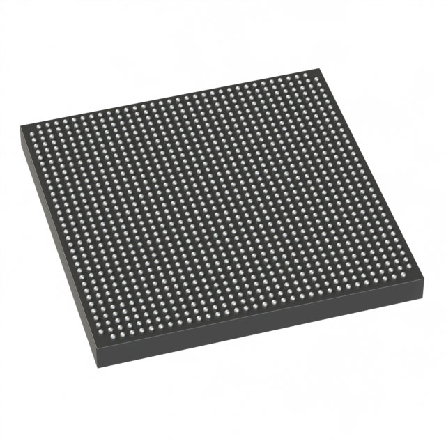
Stratix® V GX Field Programmable Gate Array (FPGA) IC 600 37888000 420000 1517-BBGA, FCBGA |
|---|---|
| Quantity | 833 Available (as of June 14, 2026) |

| Product Category | Field Programmable Gate Array (FPGA) |
|---|---|
| Manufacturer | Intel |
| Manufacturing Status | Obsolete |
| Manufacturer Standard Lead Time | Contact Us |
| Datasheet |
Specifications & Environmental
| Device Package | 1517-FBGA (40x40) | Grade | Commercial | Operating Temperature | 0°C – 85°C | ||
|---|---|---|---|---|---|---|---|
| Package / Case | 1517-BBGA, FCBGA | Number of I/O | 600 | Voltage | 870 mV - 930 mV | ||
| Mounting Method | Surface Mount | RoHS Compliance | RoHS Compliant | REACH Compliance | REACH Unknown | ||
| Moisture Sensitivity Level | 3 (168 Hours) | Number of LABs/CLBs | 158500 | Number of Logic Elements/Cells | 420000 | ||
| Number of Gates | N/A | ECCN | 3A001A2C | HTS Code | 8542.39.0001 | ||
| Qualification | N/A | Total RAM Bits | 37888000 |
Overview of 5SGXMA4K1F40C1N – Stratix® V GX FPGA, 420,000 logic elements, 600 I/Os
The 5SGXMA4K1F40C1N is a Stratix V GX field-programmable gate array (FPGA) IC from Intel (Altera). It delivers high logic density, significant on‑chip memory, and a large I/O count in a compact FCBGA package for commercial‑grade systems.
Targeted at designs that require substantial programmable logic and extensive interfacing, this device offers a combination of integration and performance characteristics suited to complex digital processing, multi‑channel I/O, and high‑density system designs.
Key Features
- Core logic capacity — 420,000 logic elements to implement large combinational and sequential designs.
- Embedded memory — approximately 37.9 Mbits of on‑chip RAM for buffering, lookup tables, and state storage.
- I/O capacity — 600 I/Os to support high channel counts and extensive peripheral interfacing.
- Power supply — core voltage range 870 mV to 930 mV for the device core supply.
- Package and mounting — 1517‑BBGA (FCBGA), supplier package 1517‑FBGA (40×40); surface‑mount package for compact board layouts.
- Temperature grade — commercial operation from 0 °C to 85 °C.
- Standards compliance — RoHS‑compliant.
- Stratix V GX family transceiver capability — the Stratix V GX family offers GX transceiver speed grades up to 14.1 Gbps according to the device datasheet.
Typical Applications
- High‑density digital signal processing — large logic capacity and substantial embedded RAM support implementation of complex DSP pipelines and algorithm acceleration.
- High‑channel I/O systems — 600 I/Os enable multi‑lane data acquisition, parallel sensor arrays, and extensive peripheral interfacing.
- Networking and communications engines — used where high logic density and the Stratix V GX family’s transceiver speed grades are needed for packet processing and protocol handling (per device family datasheet).
- Compact, high‑integration system boards — the 1517‑BBGA FCBGA package and surface‑mount mounting suit dense PCB implementations requiring a small footprint.
Unique Advantages
- High implementable logic — 420,000 logic elements reduce the need to partition designs across multiple devices, simplifying system architecture.
- Significant on‑chip memory — approximately 37.9 Mbits of embedded RAM minimizes external memory requirements for many buffering and state retention tasks.
- Extensive I/O — 600 I/Os provide flexibility for interfacing with large numbers of peripherals, sensors, and parallel data streams.
- Compact BGA packaging — 1517‑BBGA (40×40) package enables dense board layouts while keeping the device surface‑mount compatible.
- Commercial temperature operation — rated for 0 °C to 85 °C to match standard commercial system environments.
- RoHS compliant — supports regulatory needs for lead‑free assembly.
Why Choose 5SGXMA4K1F40C1N?
The 5SGXMA4K1F40C1N positions itself as a high‑capacity Stratix V GX FPGA option for commercial systems that require substantial programmable logic, large embedded memory, and wide I/O bandwidth in a compact package. Its combination of 420,000 logic elements, approximately 37.9 Mbits of on‑chip RAM, and 600 I/Os targets designs where integration density and interface count matter.
Designed and documented as part of the Stratix V family, the device benefits from the series’ technical data and configuration options. It is well suited for engineering teams building complex digital processing, high‑I/O systems, and compact boards that need a commercially graded, RoHS‑compliant FPGA solution.
Request a quote or submit an inquiry to receive pricing, availability, and lead‑time information for 5SGXMA4K1F40C1N.


Date Founded: 1968
Headquarters: Santa Clara, California, USA
Employees: 130,000+
Revenue: $54.23 Billion
Certifications and Memberships: ISO9001:2015, ISO14001:2015, ISO17025:2017, ISO27001:2022, ISO45001:2018, ISO50001:2018


