
5SGXMA4K1F40C1G
| Part Description |
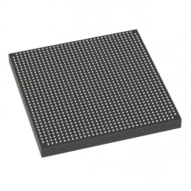
Stratix® V GX Field Programmable Gate Array (FPGA) IC 600 37888000 420000 1517-BBGA, FCBGA |
|---|---|
| Quantity | 1,064 Available (as of June 15, 2026) |

| Product Category | Field Programmable Gate Array (FPGA) |
|---|---|
| Manufacturer | Intel |
| Manufacturing Status | Active |
| Manufacturer Standard Lead Time | 26 Weeks |
| Datasheet |
Specifications & Environmental
| Device Package | 1517-FBGA (40x40) | Grade | Commercial | Operating Temperature | 0°C – 85°C | ||
|---|---|---|---|---|---|---|---|
| Package / Case | 1517-BBGA, FCBGA | Number of I/O | 600 | Voltage | 870 mV - 930 mV | ||
| Mounting Method | Surface Mount | RoHS Compliance | RoHS Compliant | REACH Compliance | REACH Unaffected | ||
| Moisture Sensitivity Level | 3 (168 Hours) | Number of LABs/CLBs | 158500 | Number of Logic Elements/Cells | 420000 | ||
| Number of Gates | N/A | ECCN | N/A | HTS Code | N/A | ||
| Qualification | N/A | Total RAM Bits | 37888000 |
Overview of 5SGXMA4K1F40C1G – Stratix® V GX FPGA, 420,000 logic elements, 600 I/O
The 5SGXMA4K1F40C1G is a Stratix® V GX field programmable gate array (FPGA) IC from Intel (Altera). It delivers very high logic density and substantial on-chip memory for designs that require large programmable logic and data buffering.
Designed as a commercial-grade device, this FCBGA-mounted FPGA targets applications that need extensive I/O capacity, large embedded RAM, and a compact surface-mount package while operating within standard commercial temperature and core-voltage ranges.
Key Features
- Core Logic Provides 420,000 logic elements for high-density programmable logic and complex implementation of digital functions.
- Embedded Memory Approximately 37.9 Mbits of on-chip RAM to support large buffers, FIFOs, and memory-intensive logic blocks.
- I/O Capacity 600 I/O pins to accommodate high-pin-count interfaces and multi-channel connectivity on a single device.
- Package & Mounting 1517-BBGA (FCBGA) / 1517-FBGA (40×40) package in a surface-mount form factor for high-density PCB integration.
- Power Supply Core voltage supply range of 870 mV to 930 mV for defined core operating conditions.
- Temperature & Grade Commercial grade with an operating temperature range of 0 °C to 85 °C.
- Regulatory Compliance RoHS compliant.
- Series Documentation Covered by the Stratix V device datasheet, which provides electrical and switching characteristics, I/O timing, and operating requirements for the Stratix V family.
Typical Applications
- High-density digital processing Use the large logic capacity to implement complex signal processing, packet processing, or custom compute pipelines on a single FPGA.
- Memory-intensive designs Approximately 37.9 Mbits of embedded RAM supports buffering, queuing, and storage requirements for data-path and protocol designs.
- High-pin-count interface systems 600 I/O pins enable aggregation of multiple interfaces, sensors, or parallel buses without external multiplexing.
- Compact, high-density boards The 1517-BBGA (FCBGA) package and surface-mount mounting facilitate dense PCB layouts where board space is constrained.
Unique Advantages
- Highly integrated logic capacity: 420,000 logic elements reduce the need for multiple devices, simplifying system architecture and lowering BOM complexity.
- Substantial embedded memory: Approximately 37.9 Mbits of on-chip RAM enables local data storage and high-throughput buffering without external memory in many designs.
- Extensive I/O resources: 600 I/O pins support broad connectivity and multi-channel interfaces directly at the FPGA, minimizing external glue logic.
- Compact FCBGA packaging: The 1517-FBGA (40×40) package provides a small footprint for high-pin-count devices, enabling compact, high-density PCB designs.
- Commercial operating window: Rated for 0 °C to 85 °C and commercial grade use, suitable for standard embedded and enterprise electronics applications.
- Standards-aligned supply and compliance: Defined core voltage range (870 mV–930 mV) and RoHS compliance support predictable power design and regulatory requirements.
Why Choose 5SGXMA4K1F40C1G?
The 5SGXMA4K1F40C1G positions itself as a high-density Stratix V GX FPGA solution for designs that demand large programmable logic, significant on-chip memory, and broad I/O capacity in a compact surface-mount package. Its commercial-grade operating range and defined core-voltage window make it suitable for a wide range of embedded and enterprise applications that require predictable electrical behavior and integration.
Engineers selecting this device gain access to the Stratix V family documentation and electrical specifications to support system design, verification, and power budgeting. The combination of logic density, embedded RAM, and extensive I/O offers a scalable platform for consolidating complex functions into a single FPGA device.
Request a quote or submit a sales inquiry to obtain pricing, lead-time, and availability information for the 5SGXMA4K1F40C1G. Our team can provide volume pricing and support for design-in requirements.


Date Founded: 1968
Headquarters: Santa Clara, California, USA
Employees: 130,000+
Revenue: $54.23 Billion
Certifications and Memberships: ISO9001:2015, ISO14001:2015, ISO17025:2017, ISO27001:2022, ISO45001:2018, ISO50001:2018


