
5SGXMA4K2F35C2WN
| Part Description |
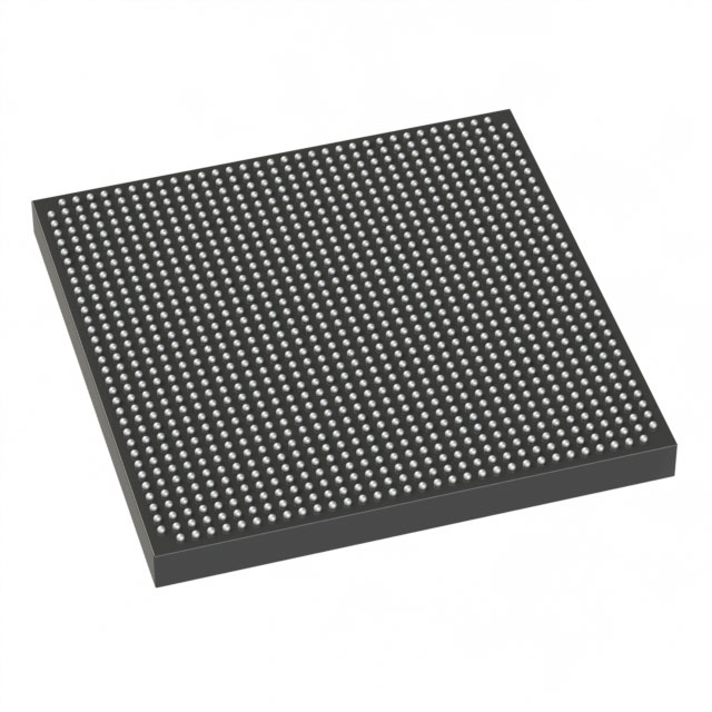
Stratix® V GX Field Programmable Gate Array (FPGA) IC 600 37888000 420000 1152-BBGA, FCBGA |
|---|---|
| Quantity | 578 Available (as of June 10, 2026) |

| Product Category | Field Programmable Gate Array (FPGA) |
|---|---|
| Manufacturer | Intel |
| Manufacturing Status | Obsolete |
| Manufacturer Standard Lead Time | Contact Us |
| Datasheet |
Specifications & Environmental
| Device Package | 1152-FBGA (35x35) | Grade | Commercial | Operating Temperature | 0°C – 85°C | ||
|---|---|---|---|---|---|---|---|
| Package / Case | 1152-BBGA, FCBGA | Number of I/O | 600 | Voltage | 870 mV - 930 mV | ||
| Mounting Method | Surface Mount | RoHS Compliance | RoHS non-compliant | REACH Compliance | REACH Unknown | ||
| Moisture Sensitivity Level | 4 (72 Hours) | Number of LABs/CLBs | 158500 | Number of Logic Elements/Cells | 420000 | ||
| Number of Gates | N/A | ECCN | OBSOLETE | HTS Code | N/A | ||
| Qualification | N/A | Total RAM Bits | 37888000 |
Overview of 5SGXMA4K2F35C2WN – Stratix® V GX FPGA, 420,000 logic elements
The 5SGXMA4K2F35C2WN is a Stratix® V GX field programmable gate array (FPGA) in a 1152‑FBGA surface‑mount package. It delivers very high logic capacity and substantial on‑chip memory for dense digital designs requiring large logic and RAM resources while operating within commercial temperature ranges.
As a member of the Stratix V GX family, this device is targeted at designs that need high integration density, abundant I/O, and tightly specified core voltage and operating conditions.
Key Features
- Logic Capacity 420,000 logic elements provide significant programmable fabric for complex digital functions and custom accelerators.
- Embedded Memory Approximately 37.9 Mbits of on‑chip RAM (37,888,000 bits) supports large buffering, LUTs, and state storage without external memory.
- I/O Resources 600 I/O pins support extensive peripheral interfacing and board-level connectivity for high‑density designs.
- Power and Core Supply Core voltage range specified at 870 mV to 930 mV to meet defined operating conditions for the device.
- Package and Mounting 1152‑FBGA (35×35) supplier package; package case listed as 1152‑BBGA, FCBGA; surface‑mount mounting type for compact board integration.
- Temperature Grade Commercial grade with an operating temperature range of 0 °C to 85 °C.
- Manufacturer and Family Intel Stratix V GX family device—electrical and switching characteristics follow the Stratix V device datasheet guidance.
- RoHS Compliant Device is RoHS compliant for environmental and regulatory considerations.
Typical Applications
- High‑density digital processing Large logic element count and extensive on‑chip RAM make the FPGA suitable for heavy compute and custom datapath implementations.
- Prototyping and system validation High logic and I/O counts enable complex system emulation and hardware prototyping on a single device.
- Interface aggregation 600 I/O pins allow aggregation and bridging of multiple interfaces within space‑constrained systems.
Unique Advantages
- High programmable capacity: 420,000 logic elements reduce the need for multi‑device partitioning on large designs.
- Large on‑chip memory: Approximately 37.9 Mbits of embedded RAM supports frame buffers, FIFOs, and state machines without immediate dependence on external memory.
- Extensive I/O availability: 600 I/Os offer flexible board‑level connectivity and peripheral support for complex systems.
- Compact, production‑ready package: 1152‑FBGA (35×35) surface‑mount packaging enables densely routed PCB layouts for volume manufacturing.
- Defined operating envelope: Commercial grade operation from 0 °C to 85 °C and a specific core voltage window (870 mV–930 mV) support predictable electrical integration.
- Vendor‑backed family: Part of the Stratix V GX family from Intel, providing alignment with documented electrical and switching characteristics.
Why Choose 5SGXMA4K2F35C2WN?
The 5SGXMA4K2F35C2WN positions itself where high logic density, substantial embedded RAM, and broad I/O capacity are required in a single commercial‑grade FPGA package. Its specification set—420,000 logic elements, approximately 37.9 Mbits of on‑chip memory, 600 I/Os, and a compact 1152‑FBGA footprint—helps simplify system architecture by consolidating functions that might otherwise need multiple devices.
This device is suitable for engineering teams developing complex digital systems, board‑level prototypes, and production products that fit within commercial temperature ranges and require a well‑defined core voltage and package form factor. Selection of this Stratix V GX FPGA leverages Intel’s Stratix V family documentation and device characterization for design and integration planning.
Request a quote or submit a procurement inquiry to receive pricing and availability for 5SGXMA4K2F35C2WN.


Date Founded: 1968
Headquarters: Santa Clara, California, USA
Employees: 130,000+
Revenue: $54.23 Billion
Certifications and Memberships: ISO9001:2015, ISO14001:2015, ISO17025:2017, ISO27001:2022, ISO45001:2018, ISO50001:2018


