
5SGXMA5H2F35I3N
| Part Description |
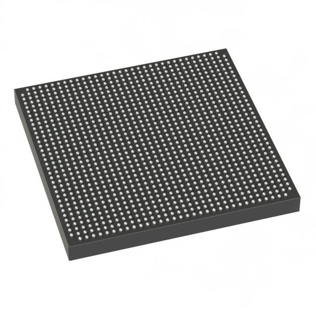
Stratix® V GX Field Programmable Gate Array (FPGA) IC 552 46080000 490000 1152-BBGA, FCBGA |
|---|---|
| Quantity | 494 Available (as of June 14, 2026) |

| Product Category | Field Programmable Gate Array (FPGA) |
|---|---|
| Manufacturer | Intel |
| Manufacturing Status | Obsolete |
| Manufacturer Standard Lead Time | Contact Us |
| Datasheet |
Specifications & Environmental
| Device Package | 1152-FBGA (35x35) | Grade | Industrial | Operating Temperature | -40°C – 100°C | ||
|---|---|---|---|---|---|---|---|
| Package / Case | 1152-BBGA, FCBGA | Number of I/O | 552 | Voltage | 820 mV - 880 mV | ||
| Mounting Method | Surface Mount | RoHS Compliance | RoHS Compliant | REACH Compliance | REACH Unknown | ||
| Moisture Sensitivity Level | 3 (168 Hours) | Number of LABs/CLBs | 185000 | Number of Logic Elements/Cells | 490000 | ||
| Number of Gates | N/A | ECCN | 3A001A2C | HTS Code | 8542.39.0001 | ||
| Qualification | N/A | Total RAM Bits | 46080000 |
Overview of 5SGXMA5H2F35I3N – Stratix® V GX Field Programmable Gate Array (FPGA) 1152-BBGA
The 5SGXMA5H2F35I3N is a Stratix V GX family FPGA in a 1152-BBGA (FCBGA) package, offered in an industrial temperature grade. It provides a large programmable fabric and peripheral resources for designs requiring substantial logic capacity, dense I/O, and on-chip embedded memory.
Key device attributes include approximately 490,000 logic elements (documented as 185,000 logic blocks), roughly 46 Mbits of embedded memory, and 552 I/O pins—making the device suitable for complex, memory- and I/O-heavy programmable logic implementations that must operate across a –40 °C to 100 °C temperature range.
Key Features
- Logic Capacity Approximately 490,000 logic elements, corresponding to the part’s large programmable fabric for implementing complex digital functions.
- Embedded Memory Approximately 46 Mbits of on-chip RAM (46,080,000 total RAM bits) to support buffering, large state machines, and memory-intensive processing.
- High I/O Count 552 general-purpose I/O pins to support dense external interfacing and multi-channel connectivity.
- Industrial Temperature Grade Rated for operation from –40 °C to 100 °C to meet industrial application environmental requirements.
- Low-Voltage Core Core voltage supply specified between 820 mV and 880 mV for the device core power domain.
- Package and Mounting 1152-BBGA (supplier package: 1152-FBGA, 35×35) in a surface-mount FCBGA format for high-pin-count board designs.
- Regulatory Compliance RoHS compliant.
Typical Applications
- High-density digital logic Implement large custom state machines, datapaths, and protocol engines using the device’s ~490,000 logic elements and extensive on-chip RAM.
- Memory-intensive processing Leverage approximately 46 Mbits of embedded memory for buffering, packet processing, and data aggregation tasks.
- Dense I/O systems Use 552 I/O pins to connect to multiple peripherals, high-channel-count front-ends, or parallel interfaces in industrial systems.
- Industrial embedded systems Deploy in applications requiring operation across –40 °C to 100 °C, benefiting from the device’s industrial grade and surface-mount FCBGA package.
Unique Advantages
- Large programmable fabric: Enables integration of complex logic and multiple functions into a single device, reducing board-level component count.
- Substantial embedded memory: Approximately 46 Mbits of on-chip RAM reduces dependence on external memory for many buffering and data-path tasks.
- Extensive I/O availability: 552 I/O pins support high channel counts and flexible interfacing without immediate need for I/O expanders.
- Industrial temperature rating: Operation from –40 °C to 100 °C supports deployment in harsh or temperature-variable environments.
- Compact high-pin-count package: 1152-BBGA (35×35 FCBGA) provides a dense, surface-mount solution for space-constrained PCBs while preserving routing density.
- Standards-aligned supply domain: Core voltage specified at 820–880 mV enables integration with modern low-voltage power architectures.
Why Choose 5SGXMA5H2F35I3N?
The 5SGXMA5H2F35I3N delivers a combination of large logic capacity, significant embedded memory, and a high I/O count in an industrial-grade Stratix V GX FPGA. These attributes make it well suited for designers who need to consolidate complex digital functions, support memory-heavy data paths, and interface to many external signals within a single programmable device.
For engineering teams targeting demanding embedded and industrial applications, this FPGA offers a scalable, high-density platform with a proven device family foundation and specifications that support robust, long-term deployments.
Request a quote or submit a purchase inquiry to discuss availability, pricing, and lead time for the 5SGXMA5H2F35I3N.


Date Founded: 1968
Headquarters: Santa Clara, California, USA
Employees: 130,000+
Revenue: $54.23 Billion
Certifications and Memberships: ISO9001:2015, ISO14001:2015, ISO17025:2017, ISO27001:2022, ISO45001:2018, ISO50001:2018


