
5SGXMA5K2F40I3NAA
| Part Description |
Stratix® V GX Field Programmable Gate Array (FPGA) IC 696 46080000 490000 1517-BBGA, FCBGA |
|---|---|
| Quantity | 27 Available (as of June 15, 2026) |

| Product Category | Field Programmable Gate Array (FPGA) |
|---|---|
| Manufacturer | Intel |
| Manufacturing Status | Obsolete |
| Manufacturer Standard Lead Time | Contact Us |
| Datasheet |
Specifications & Environmental
| Device Package | 1517-FBGA (40x40) | Grade | Industrial | Operating Temperature | -40°C – 100°C | ||
|---|---|---|---|---|---|---|---|
| Package / Case | 1517-BBGA, FCBGA | Number of I/O | 696 | Voltage | 820 mV - 880 mV | ||
| Mounting Method | Surface Mount | RoHS Compliance | RoHS non-compliant | REACH Compliance | REACH Unknown | ||
| Moisture Sensitivity Level | 4 (72 Hours) | Number of LABs/CLBs | 185000 | Number of Logic Elements/Cells | 490000 | ||
| Number of Gates | N/A | ECCN | OBSOLETE | HTS Code | N/A | ||
| Qualification | N/A | Total RAM Bits | 46080000 |
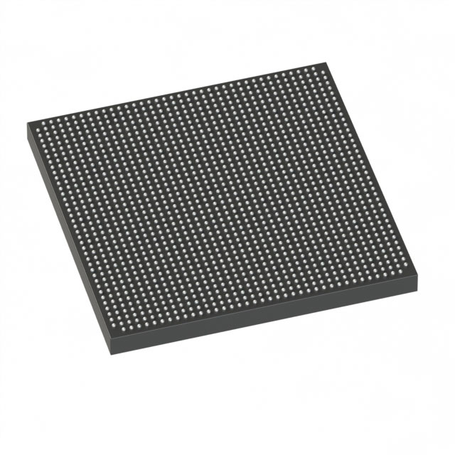
Overview of 5SGXMA5K2F40I3NAA – Stratix® V GX FPGA, 490,000 logic elements, 1517-BBGA
The 5SGXMA5K2F40I3NAA is a Stratix® V GX Field Programmable Gate Array (FPGA) IC from Intel. It provides a high-density, configurable logic fabric combined with large embedded memory and a very high I/O count for demanding digital designs.
This device is positioned for systems that require substantial on-chip logic and memory capacity, extensive external connectivity, and industrial-temperature operation. Key value propositions include large logic capacity, significant embedded RAM, and broad I/O resources in a compact surface-mount BGA package.
Key Features
- Core logic Approximately 490,000 logic elements to implement complex digital functions and custom accelerators.
- Embedded memory Approximately 46.08 Mbits of on-chip RAM to support buffering, caches, and memory-intensive algorithms.
- I/O capacity 696 I/O pins to support wide parallel interfaces, multiple high-speed links, and extensive peripheral connectivity.
- Transceiver grades (series-level) Stratix V GX devices include GX transceiver speed grades (series datasheet lists GX channel capabilities up to 14.1 Gbps), enabling high-speed serial communications at the family level.
- Power and core supply Core voltage supply range 0.820 V to 0.880 V for the device’s core power domain.
- Package & mounting 1517-BBGA (FCBGA) package, supplier device package 1517-FBGA (40×40), designed for surface-mount assembly.
- Industrial temperature grade Rated for operation from −40 °C to 100 °C for use in industrial environments.
- RoHS compliant Device meets RoHS environmental compliance requirements.
Typical Applications
- High-speed communications System designs that leverage the Stratix V GX family transceiver grades and the device’s high I/O count for backplane, switch, or serial link interfaces.
- Compute acceleration and DSP FPGA-based accelerators and signal-processing engines that benefit from the large logic element count and substantial on-chip RAM.
- Industrial control and instrumentation Control systems and instrumentation that require industrial temperature operation (−40 °C to 100 °C) and high integration density.
- Prototype and system integration Complex prototypes and multi-function systems that need many I/Os and a high-density BGA package for compact board layouts.
Unique Advantages
- High logic density: Approximately 490,000 logic elements enable implementation of large, complex designs on a single device.
- Substantial embedded memory: Approximately 46.08 Mbits of on-chip RAM reduces dependence on external memory for many workloads.
- Extensive I/O resources: 696 I/Os simplify board-level design by supporting multiple interfaces and parallel connectivity without excessive external logic.
- Industrial temperature rating: −40 °C to 100 °C operation supports deployment in harsher environments.
- Low-voltage core operation: 0.820–0.880 V core supply supports core-power optimization strategies.
- Industry-standard package: 1517-BBGA (40×40 FCBGA) surface-mount package for compact, production-ready assemblies.
Why Choose 5SGXMA5K2F40I3NAA?
The 5SGXMA5K2F40I3NAA delivers a combination of high logic capacity, significant on-chip memory, and a large I/O footprint in an industrial-temperature Stratix V GX FPGA. It is well suited to designers building high-performance communications, compute acceleration, and industrial systems that need dense logic and ample embedded RAM in a production-ready BGA package.
As a member of the Stratix V GX family, this device provides series-level transceiver capabilities and device-level specifications that support scalable designs where integration density, I/O breadth, and temperature robustness are important considerations.
Request a quote or submit an inquiry to obtain pricing and availability for 5SGXMA5K2F40I3NAA. Our team can provide ordering and lead-time information to support your design schedule.


Date Founded: 1968
Headquarters: Santa Clara, California, USA
Employees: 130,000+
Revenue: $54.23 Billion
Certifications and Memberships: ISO9001:2015, ISO14001:2015, ISO17025:2017, ISO27001:2022, ISO45001:2018, ISO50001:2018


