
5SGXMA7H2F35C3N
| Part Description |
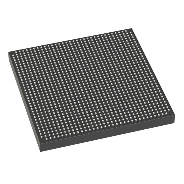
Stratix® V GX Field Programmable Gate Array (FPGA) IC 552 51200000 622000 1152-BBGA, FCBGA |
|---|---|
| Quantity | 438 Available (as of June 15, 2026) |

| Product Category | Field Programmable Gate Array (FPGA) |
|---|---|
| Manufacturer | Intel |
| Manufacturing Status | Obsolete |
| Manufacturer Standard Lead Time | Contact Us |
| Datasheet |
Specifications & Environmental
| Device Package | 1152-FBGA (35x35) | Grade | Commercial | Operating Temperature | 0°C – 85°C | ||
|---|---|---|---|---|---|---|---|
| Package / Case | 1152-BBGA, FCBGA | Number of I/O | 552 | Voltage | 870 mV - 930 mV | ||
| Mounting Method | Surface Mount | RoHS Compliance | RoHS Compliant | REACH Compliance | REACH Unknown | ||
| Moisture Sensitivity Level | 3 (168 Hours) | Number of LABs/CLBs | 234720 | Number of Logic Elements/Cells | 622000 | ||
| Number of Gates | N/A | ECCN | 3A001A2C | HTS Code | 8542.39.0001 | ||
| Qualification | N/A | Total RAM Bits | 51200000 |
Overview of 5SGXMA7H2F35C3N – Stratix® V GX Field Programmable Gate Array, 1152‑BBGA
The 5SGXMA7H2F35C3N is a Stratix® V GX Field Programmable Gate Array (FPGA) IC designed for high‑density commercial applications. The device integrates a large logic fabric, substantial embedded memory, and extensive I/O to support complex digital designs.
Key on‑chip resources include 622,000 logic elements, approximately 51.2 Mbits of embedded memory, and up to 552 I/O pins. The device is supplied in a 1152‑ball FCBGA (35×35) package and is rated for commercial operation from 0 °C to 85 °C.
Key Features
- Core Logic Capacity Provides 622,000 logic elements to implement large, complex digital systems and multi‑function designs.
- Embedded Memory Approximately 51.2 Mbits of on‑chip RAM for buffering, packet processing, and on‑device data storage.
- I/O Density Up to 552 I/O pins to support wide parallel interfaces and high port counts for system integration.
- Power and Voltage Core supply operating range of 0.870 V to 0.930 V to match targeted power rails and design constraints.
- Package and Mounting 1152‑BBGA (FCBGA) supplier package, 35×35 mm, surface‑mount for compact board‑level integration.
- Operating Range Commercial temperature grade with an operating range of 0 °C to 85 °C.
- Environmental Compliance RoHS compliant for regulatory and manufacturing alignment.
Typical Applications
- High‑density digital systems Implement complex logic functions and state machines using the large pool of logic elements and on‑chip RAM.
- Networking and communications equipment Support for wide I/O counts and embedded memory makes the device suitable for packet buffering and protocol handling in commercial networking gear.
- Data processing and acceleration On‑chip memory and extensive logic allow for hardware acceleration of data paths and processing kernels in embedded platforms.
- FPGA‑based prototyping and system integration High logic capacity and I/O flexibility enable board‑level prototyping and integration of multi‑interface designs.
Unique Advantages
- High logic density: 622,000 logic elements provide headroom for large designs and multi‑core implementations.
- Substantial embedded memory: Approximately 51.2 Mbits of on‑chip RAM reduces external memory dependency for many buffering and storage needs.
- Extensive I/O connectivity: Up to 552 I/O pins support multiple parallel interfaces and complex system interconnects.
- Compact, production‑ready package: 1152‑BBGA (FCBGA) surface‑mount package enables high‑density PCB layouts.
- Defined power envelope: Core voltage range of 0.870–0.930 V helps integration with targeted power supplies and power management designs.
- Commercial temperature and RoHS compliance: Rated for 0 °C to 85 °C and RoHS compliant for commercial production environments.
Why Choose 5SGXMA7H2F35C3N?
The 5SGXMA7H2F35C3N positions itself as a high‑capacity Stratix V GX FPGA for commercial applications where large logic count, significant embedded memory, and broad I/O are required. Its 1152‑ball FCBGA package and surface‑mount form factor support compact system designs while the defined core voltage and commercial temperature rating simplify integration into production boards.
This part is well suited for engineering teams building complex FPGA‑based systems that require on‑device memory, high I/O counts, and a production‑grade surface‑mount package backed by Stratix V family documentation.
Request a quote or submit a purchase inquiry referencing part number 5SGXMA7H2F35C3N to begin sourcing this Stratix® V GX FPGA for your design.


Date Founded: 1968
Headquarters: Santa Clara, California, USA
Employees: 130,000+
Revenue: $54.23 Billion
Certifications and Memberships: ISO9001:2015, ISO14001:2015, ISO17025:2017, ISO27001:2022, ISO45001:2018, ISO50001:2018


