
5SGXMA7K3F35C4
| Part Description |
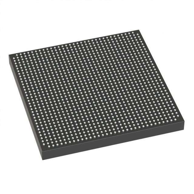
Stratix® V GX Field Programmable Gate Array (FPGA) IC 432 51200000 622000 1152-BBGA, FCBGA |
|---|---|
| Quantity | 832 Available (as of June 18, 2026) |

| Product Category | Field Programmable Gate Array (FPGA) |
|---|---|
| Manufacturer | Intel |
| Manufacturing Status | Obsolete |
| Manufacturer Standard Lead Time | Contact Us |
| Datasheet |
Specifications & Environmental
| Device Package | 1152-FBGA (35x35) | Grade | Commercial | Operating Temperature | 0°C – 85°C | ||
|---|---|---|---|---|---|---|---|
| Package / Case | 1152-BBGA, FCBGA | Number of I/O | 432 | Voltage | 820 mV - 880 mV | ||
| Mounting Method | Surface Mount | RoHS Compliance | RoHS Compliant | REACH Compliance | REACH Unknown | ||
| Moisture Sensitivity Level | 3 (168 Hours) | Number of LABs/CLBs | 234720 | Number of Logic Elements/Cells | 622000 | ||
| Number of Gates | N/A | ECCN | 3A001A2C | HTS Code | 8542.39.0001 | ||
| Qualification | N/A | Total RAM Bits | 51200000 |
Overview of 5SGXMA7K3F35C4 – Stratix® V GX FPGA, 622,000 logic elements, 432 I/O, 1152-BBGA
The 5SGXMA7K3F35C4 is a Stratix V GX Field Programmable Gate Array (FPGA) from Intel. It delivers a high-density programmable fabric with approximately 622,000 logic elements and approximately 51.2 Mbits of embedded memory for complex digital integration.
Designed as a surface-mount 1152-BBGA FCBGA device, this commercial-grade FPGA provides 432 I/O pins, a core supply range of 820 mV to 880 mV, and an operating temperature range of 0 °C to 85 °C. It is RoHS compliant and targeted at applications that require substantial on-chip logic, memory, and I/O capacity.
Key Features
- Core Logic Approximately 622,000 logic elements to implement large-scale digital designs and deep custom logic blocks.
- Embedded Memory Approximately 51.2 Mbits of on-chip RAM for buffering, state storage, and memory-intensive algorithms.
- I/O Density 432 general-purpose I/O pins to support wide parallel interfaces and extensive peripheral connectivity.
- Transceiver Capability (Stratix V GX family) Stratix V GX devices support transceiver speed grades described in the family datasheet (for example, GX channel speed grades up to 14.1 Gbps as documented for the series).
- Power and Operating Conditions Core voltage supply range from 820 mV to 880 mV and commercial operating temperature from 0 °C to 85 °C for standard environment deployments.
- Package & Mounting 1152-BBGA FCBGA package; supplier device package listed as 1152-FBGA (35×35). Surface-mount mounting type for PCB assembly.
- Regulatory RoHS compliant.
Typical Applications
- High-density FPGA designs Implement large custom logic networks and complex state machines using the device's approximately 622,000 logic elements.
- Memory-intensive functions Leverage approximately 51.2 Mbits of embedded memory for buffering, packet storage, or algorithmic working memory.
- High I/O systems Use the 432 I/O pins to interface with parallel buses, sensor arrays, or multi-channel I/O subsystems.
- High-speed serial systems (family-level) For designs that utilize Stratix V GX transceivers, the family-level transceiver speed grades support high-bandwidth serial links as documented in the Stratix V device specifications.
Unique Advantages
- High on-chip integration: With approximately 622,000 logic elements and ~51.2 Mbits of embedded memory, the device enables consolidation of functions that might otherwise require multiple components.
- Large I/O footprint: 432 I/O pins give designers flexibility to connect multiple parallel interfaces without extensive external switching.
- Commercial temperature grade: Rated for 0 °C to 85 °C operation, suitable for standard commercial deployments.
- Compact surface-mount package: 1152-BBGA FCBGA packaging provides a high-pin-count solution in a compact form factor appropriate for dense PCB layouts.
- Standards-conscious manufacturing: RoHS compliance supports environmentally conscious assembly and regulatory requirements.
Why Choose 5SGXMA7K3F35C4?
The 5SGXMA7K3F35C4 places substantial programmable resources—approximately 622,000 logic elements and roughly 51.2 Mbits of embedded RAM—into a single commercial-grade Stratix V GX device. Its combination of high logic density, significant on-chip memory, and 432 I/O pins makes it suitable for complex FPGA-based systems that need to integrate multiple functions on a single silicon device.
As a member of the Stratix V GX family, this device is documented in the Stratix V device specifications, which describe electrical characteristics, operating conditions, and family-level transceiver capabilities. That documentation supports design planning where large logic capacity, abundant memory, and wide I/O are primary requirements.
Request a quote or submit a purchase inquiry to evaluate 5SGXMA7K3F35C4 for your next high-density FPGA design.


Date Founded: 1968
Headquarters: Santa Clara, California, USA
Employees: 130,000+
Revenue: $54.23 Billion
Certifications and Memberships: ISO9001:2015, ISO14001:2015, ISO17025:2017, ISO27001:2022, ISO45001:2018, ISO50001:2018


