
5SGXMA7N2F45C2LN
| Part Description |
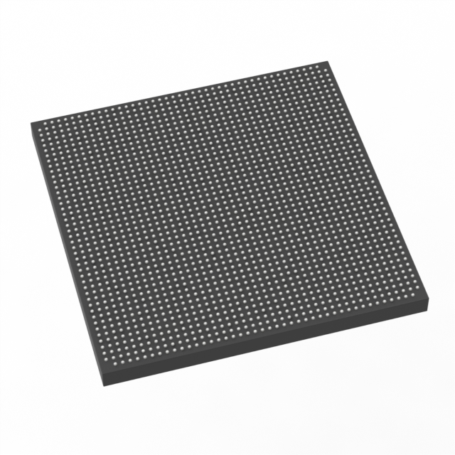
Stratix® V GX Field Programmable Gate Array (FPGA) IC 840 51200000 622000 1932-BBGA, FCBGA |
|---|---|
| Quantity | 831 Available (as of June 14, 2026) |

| Product Category | Field Programmable Gate Array (FPGA) |
|---|---|
| Manufacturer | Intel |
| Manufacturing Status | Obsolete |
| Manufacturer Standard Lead Time | Contact Us |
| Datasheet |
Specifications & Environmental
| Device Package | 1932-FBGA, FC (45x45) | Grade | Commercial | Operating Temperature | 0°C – 85°C | ||
|---|---|---|---|---|---|---|---|
| Package / Case | 1932-BBGA, FCBGA | Number of I/O | 840 | Voltage | 820 mV - 880 mV | ||
| Mounting Method | Surface Mount | RoHS Compliance | RoHS Compliant | REACH Compliance | REACH Unknown | ||
| Moisture Sensitivity Level | 3 (168 Hours) | Number of LABs/CLBs | 234720 | Number of Logic Elements/Cells | 622000 | ||
| Number of Gates | N/A | ECCN | 3A001A2C | HTS Code | 8542.39.0001 | ||
| Qualification | N/A | Total RAM Bits | 51200000 |
Overview of 5SGXMA7N2F45C2LN – Stratix V GX FPGA, 622,000 logic elements
The 5SGXMA7N2F45C2LN is an Intel Stratix V GX field programmable gate array (FPGA) supplied in a 1932-pin FCBGA package for surface-mount assembly. It delivers high on-chip logic density and embedded memory with a large I/O count to support complex digital designs.
Designed for commercial-temperature applications, this device targets designs that require substantial logic capacity, significant embedded RAM, and extensive I/O connectivity while operating within a core voltage range of 820 mV to 880 mV.
Key Features
- Logic Density 622,000 logic elements provide substantial resources for implementing large digital systems and complex algorithms.
- Embedded Memory Approximately 51.2 Mbits of on-chip RAM to support buffering, data storage, and high-throughput processing on chip.
- I/O Capacity 840 I/Os to support extensive peripheral connectivity, parallel interfaces, and board-level integration.
- Core Architecture & Speed Grades Stratix V GX family characteristics are reflected in this part’s architecture; consult the device datasheet for details on available speed grades and transceiver options.
- Power and Voltage Core voltage supply range of 820 mV to 880 mV for the FPGA core domain.
- Package & Mounting 1932-BBGA (FCBGA) package case; supplier device package listed as 1932-FBGA, FC (45x45). Surface-mount mounting type.
- Operating Range & Grade Commercial grade device with an operating temperature range of 0 °C to 85 °C.
- Compliance RoHS compliant.
Typical Applications
- High-density digital systems — Implement complex FPGA designs that require hundreds of thousands of logic elements and large embedded RAM capacity.
- Multi-interface platforms — Use the large I/O count to aggregate parallel and serial interfaces on a single device.
- Memory-intensive processing — Deploy approximately 51.2 Mbits of on-chip RAM for buffering, packet processing, and temporary data storage.
Unique Advantages
- Substantial logic capacity: 622,000 logic elements enable large-scale integration of digital functions without immediate reliance on external logic chips.
- Significant on-chip memory: Approximately 51.2 Mbits of embedded RAM reduces external memory bandwidth needs and simplifies board-level memory design.
- High I/O count: 840 I/Os provide flexibility for dense connector and peripheral configurations, minimizing the need for external I/O expanders.
- Commercial temperature fit: Rated for 0 °C to 85 °C operation for deployments in commercial-grade systems and environments.
- Surface-mount FCBGA package: 1932-BBGA package supports compact board layouts and automated assembly processes.
- Regulatory alignment: RoHS compliance supports environmentally conscious designs and supply-chain requirements.
Why Choose 5SGXMA7N2F45C2LN?
The 5SGXMA7N2F45C2LN combines high logic density, substantial embedded RAM, and a large I/O complement in a single commercial-grade Stratix V GX FPGA package. It is well-suited to designers who need to consolidate complex digital functions, memory buffering, and extensive interfacing into one programmable device while operating in standard commercial environments.
This part offers a balance of integration and scalability for medium- to high-complexity FPGA designs. Its package and mounting support production-ready surface-mount assembly, and RoHS compliance helps meet modern environmental requirements.
Request a quote or submit a parts inquiry to obtain pricing and availability for 5SGXMA7N2F45C2LN. Provide your quantity and any required delivery or packaging details to receive a prompt response.


Date Founded: 1968
Headquarters: Santa Clara, California, USA
Employees: 130,000+
Revenue: $54.23 Billion
Certifications and Memberships: ISO9001:2015, ISO14001:2015, ISO17025:2017, ISO27001:2022, ISO45001:2018, ISO50001:2018


