
5SGXMA9K1H40C2LG
| Part Description |
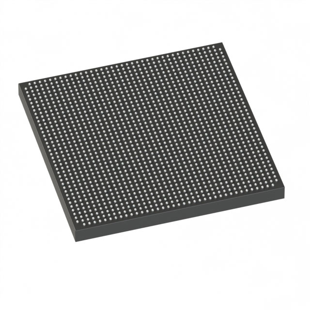
Stratix® V GX Field Programmable Gate Array (FPGA) IC 696 53248000 840000 1517-BBGA, FCBGA |
|---|---|
| Quantity | 523 Available (as of June 14, 2026) |

| Product Category | Field Programmable Gate Array (FPGA) |
|---|---|
| Manufacturer | Intel |
| Manufacturing Status | Active |
| Manufacturer Standard Lead Time | 26 Weeks |
| Datasheet |
Specifications & Environmental
| Device Package | 1517-HBGA (45x45) | Grade | Commercial | Operating Temperature | 0°C – 85°C | ||
|---|---|---|---|---|---|---|---|
| Package / Case | 1517-BBGA, FCBGA | Number of I/O | 696 | Voltage | 820 mV - 880 mV | ||
| Mounting Method | Surface Mount | RoHS Compliance | RoHS Compliant | REACH Compliance | REACH Unaffected | ||
| Moisture Sensitivity Level | 3 (168 Hours) | Number of LABs/CLBs | 317000 | Number of Logic Elements/Cells | 840000 | ||
| Number of Gates | N/A | ECCN | N/A | HTS Code | N/A | ||
| Qualification | N/A | Total RAM Bits | 53248000 |
Overview of 5SGXMA9K1H40C2LG – Stratix® V GX FPGA, 840,000 logic elements, ~53.25 Mbits RAM, 696 I/Os, 1517-BBGA
The 5SGXMA9K1H40C2LG is an Intel Stratix® V GX field-programmable gate array (FPGA) delivering high logic density and on-chip memory in a commercial-temperature, surface-mount package. As a GX-class Stratix V device, it is designed for designs that require large programmable logic capacity, substantial embedded memory, and a high I/O count for complex system integration.
With 840,000 logic elements, approximately 53.25 Mbits of embedded memory, and 696 I/Os, this device targets demanding computational and connectivity use cases where integration, channel density, and routing flexibility matter.
Key Features
- Core Logic 840,000 logic elements provide extensive programmable resources for large-scale logic, control, and custom hardware acceleration.
- Embedded Memory Approximately 53.25 Mbits of on-chip RAM to support buffering, on-device data storage, and memory-intensive algorithms.
- I/O Density 696 I/Os enable high channel counts and flexible interfacing options for parallel and serial connectivity.
- Package & Mounting 1517-BBGA (FCBGA) package; supplier device package 1517-HBGA (45×45); surface-mount mounting for PCB integration.
- Power Core supply range specified at 820 mV to 880 mV to match platform power planning and voltage-rail design.
- Operating Grade Commercial grade with an operating temperature range of 0 °C to 85 °C for standard commercial environments.
- Regulatory RoHS compliant for environmental and manufacturing compliance requirements.
Typical Applications
- High-density programmable logic Large-scale logic implementations and hardware-accelerated functions that require a high count of logic elements and embedded memory.
- High-channel I/O systems Boards and systems that need many external interfaces or parallel I/O channels, leveraging the 696 available I/Os.
- Custom compute and DSP On-device memory and extensive logic resources for signal processing kernels, streaming pipelines, and custom accelerators.
- Prototype and advanced FPGA development Platform-level FPGA designs where density, integration, and flexibility are priorities during development and verification.
Unique Advantages
- High logic density: 840,000 logic elements enable integration of large digital designs on a single device, reducing board-level component count.
- Substantial embedded memory: Approximately 53.25 Mbits of on-chip RAM supports deep buffering and on-chip data structures without immediate external memory needs.
- Extensive I/O count: 696 I/Os simplify complex system interconnects and reduce the need for external multiplexing or IO expansion.
- Commercial-grade thermal range: Rated 0 °C to 85 °C for deployments in standard commercial environments and controlled enclosures.
- Compact, surface-mount package: 1517-BBGA (1517-HBGA supplier package, 45×45) provides a dense physical footprint suitable for PCB integration.
- RoHS compliant: Meets environmental compliance requirements for manufacturing and supply chain considerations.
Why Choose 5SGXMA9K1H40C2LG?
The 5SGXMA9K1H40C2LG positions itself as a high-density, commercial-grade Stratix V GX FPGA option for designs that need extensive programmable logic, significant on-chip memory, and a high I/O complement in a compact FCBGA package. Its specified core voltage range and surface-mount package simplify power and board design for medium- to large-scale FPGA implementations.
This device is well suited to engineering teams building compute-heavy, I/O-rich systems where integrating large amounts of logic and memory on a single device reduces system complexity and BOM count. Intel’s Stratix V GX family device characteristics provide a clear development path for projects requiring scalable programmable-capacity within commercial temperature operation.
Request a quote or submit a pricing inquiry to receive availability, lead-time, and quantity pricing for the 5SGXMA9K1H40C2LG.


Date Founded: 1968
Headquarters: Santa Clara, California, USA
Employees: 130,000+
Revenue: $54.23 Billion
Certifications and Memberships: ISO9001:2015, ISO14001:2015, ISO17025:2017, ISO27001:2022, ISO45001:2018, ISO50001:2018


