
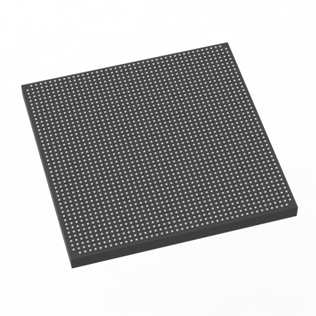
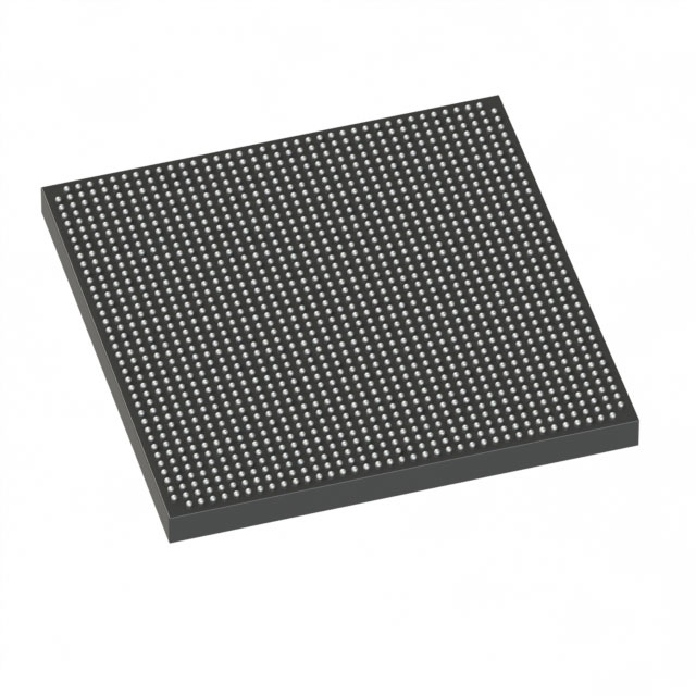
5SGXMA7N3F45I4G
| Part Description |
Stratix® V GX Field Programmable Gate Array (FPGA) IC 840 51200000 622000 1932-BBGA, FCBGA |
|---|---|
| Quantity | 216 Available (as of June 17, 2026) |

| Product Category | Field Programmable Gate Array (FPGA) |
|---|---|
| Manufacturer | Intel |
| Manufacturing Status | Active |
| Manufacturer Standard Lead Time | 26 Weeks |
| Datasheet |
Specifications & Environmental
| Device Package | 1932-FBGA, FC (45x45) | Grade | Industrial | Operating Temperature | -40°C – 100°C | ||
|---|---|---|---|---|---|---|---|
| Package / Case | 1932-BBGA, FCBGA | Number of I/O | 840 | Voltage | 820 mV - 880 mV | ||
| Mounting Method | Surface Mount | RoHS Compliance | RoHS Compliant | REACH Compliance | REACH Unaffected | ||
| Moisture Sensitivity Level | 3 (168 Hours) | Number of LABs/CLBs | 234720 | Number of Logic Elements/Cells | 622000 | ||
| Number of Gates | N/A | ECCN | N/A | HTS Code | N/A | ||
| Qualification | N/A | Total RAM Bits | 51200000 |
Overview of 5SGXMA7N3F45I4G – Stratix® V GX FPGA (High-density, Industrial-grade)
The 5SGXMA7N3F45I4G is an Intel Stratix V GX Field Programmable Gate Array (FPGA) supplied in a 1932-BBGA FCBGA package. It delivers large on-chip logic and memory resources alongside a substantial I/O count, making it suitable for demanding industrial applications that require high integration and extended temperature operation.
With 622,000 logic elements, approximately 51.2 Mbits of embedded memory and 840 user I/Os, this device targets designs that need high-density programmable logic, significant embedded storage, and broad interfacing capability within a compact surface-mount package.
Key Features
- Core & Logic 622,000 logic elements for high-density programmable logic and complex digital designs.
- Embedded Memory Approximately 51.2 Mbits of on-chip RAM to support large buffers, state machines and local data storage.
- I/O Capacity 840 user I/Os to accommodate extensive external interfacing and system-level connectivity.
- Power Supply Core supply range of 820 mV to 880 mV for the device core voltage domain.
- Package & Mounting 1932-BBGA (FCBGA) package, supplier device package listed as 1932-FBGA, FC (45×45), designed for surface-mount assembly.
- Temperature & Grade Industrial grade with an operating temperature range of −40°C to 100°C for use in extended-temperature environments.
- Compliance RoHS compliant, supporting regulatory requirements for lead-free assemblies.
Typical Applications
- Industrial Control Systems High logic density and extended temperature range support complex control algorithms and robust field deployment.
- High-throughput Data Processing Large on-chip RAM and extensive logic resources enable buffering and parallel processing for data-centric applications.
- Signal Processing and Acceleration Substantial logic and memory allow implementation of custom accelerators and DSP pipelines within the FPGA fabric.
- Complex I/O and Interface Bridging 840 I/Os simplify integration with multiple peripherals, sensors and external subsystems in compact system designs.
Unique Advantages
- Highly integrated logic and memory: 622,000 logic elements combined with approximately 51.2 Mbits of embedded RAM reduce the need for external components and simplify system architecture.
- Broad system interfacing: 840 user I/Os enable rich peripheral connectivity and flexible board-level integration.
- Industrial temperature range: Rated for −40°C to 100°C operation to support deployment in temperature-challenging environments.
- Compact, surface-mount FCBGA package: 1932-BBGA/1932-FBGA packaging provides high density in a board-level footprint optimized for modern assemblies.
- Low-voltage core operation: 820 mV to 880 mV supply range for the core domain, enabling designs that target optimized power rails.
- Regulatory readiness: RoHS compliance helps meet lead-free manufacturing requirements.
Why Choose 5SGXMA7N3F45I4G?
The 5SGXMA7N3F45I4G positions itself as a high-density, industrial-grade Stratix V GX FPGA that balances large programmable logic resources, significant embedded memory and a high I/O count within a compact FCBGA package. These characteristics make it well suited for developers and systems integrators building complex, reliability-focused designs that require substantial on-chip resources and robust thermal performance.
For projects that demand scalability of logic and memory, extensive peripheral connectivity and compliance with RoHS and industrial temperature requirements, this device provides a clear, specification-driven foundation for both prototype and production deployments.
Request a quote or submit an inquiry for pricing and availability to begin integrating the 5SGXMA7N3F45I4G into your next design.


Date Founded: 1968
Headquarters: Santa Clara, California, USA
Employees: 130,000+
Revenue: $54.23 Billion
Certifications and Memberships: ISO9001:2015, ISO14001:2015, ISO17025:2017, ISO27001:2022, ISO45001:2018, ISO50001:2018


