
5SGXMA7N3F45I3WN
| Part Description |
Stratix® V GX Field Programmable Gate Array (FPGA) IC 840 51200000 622000 1932-BBGA, FCBGA |
|---|---|
| Quantity | 587 Available (as of June 12, 2026) |

| Product Category | Field Programmable Gate Array (FPGA) |
|---|---|
| Manufacturer | Intel |
| Manufacturing Status | Obsolete |
| Manufacturer Standard Lead Time | Contact Us |
| Datasheet |
Specifications & Environmental
| Device Package | 1932-FBGA, FC (45x45) | Grade | Industrial | Operating Temperature | -40°C – 100°C | ||
|---|---|---|---|---|---|---|---|
| Package / Case | 1932-BBGA, FCBGA | Number of I/O | 840 | Voltage | 820 mV - 880 mV | ||
| Mounting Method | Surface Mount | RoHS Compliance | RoHS non-compliant | REACH Compliance | REACH Unknown | ||
| Moisture Sensitivity Level | 4 (72 Hours) | Number of LABs/CLBs | 234720 | Number of Logic Elements/Cells | 622000 | ||
| Number of Gates | N/A | ECCN | OBSOLETE | HTS Code | N/A | ||
| Qualification | N/A | Total RAM Bits | 51200000 |
Overview of 5SGXMA7N3F45I3WN – Stratix® V GX Field Programmable Gate Array (FPGA)
The 5SGXMA7N3F45I3WN is a Stratix V GX FPGA from Intel, delivered in a high-density 1932-BBGA FCBGA package. It provides a large logic fabric and sizable on-chip memory for designs that require substantial programmable logic, extensive I/O, and industrial-temperature operation.
With 622,000 logic elements, approximately 51.2 Mbits of embedded memory, and 840 I/O pins, this device targets complex digital processing and high‑integration system designs while operating across an industrial temperature range and a nominal core supply window.
Key Features
- Logic Capacity 622,000 logic elements (cells) to support large, complex FPGA designs and dense logic implementations.
- Embedded Memory Approximately 51.2 Mbits of on‑chip RAM for buffering, lookup tables, and data storage close to the logic fabric.
- I/O Integration 840 programmable I/O pins to interface with high‑pin‑count systems and multiple peripheral domains.
- Power Supply Core voltage support in the range 820 mV to 880 mV for compatibility with targeted Stratix V power domains.
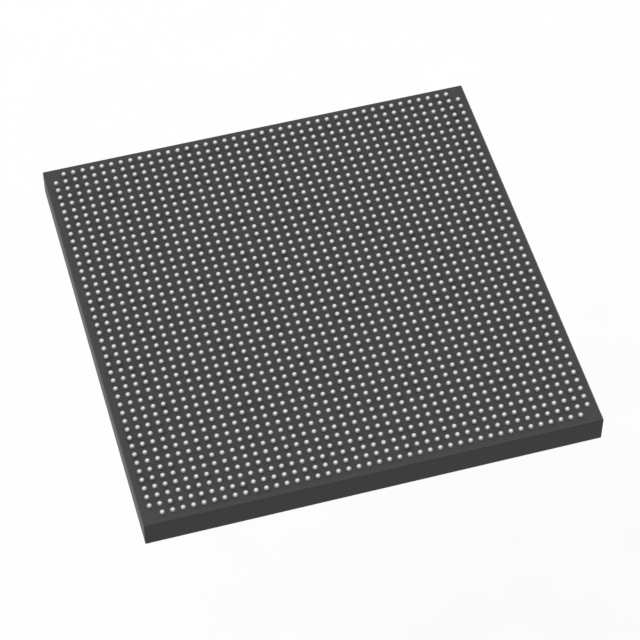
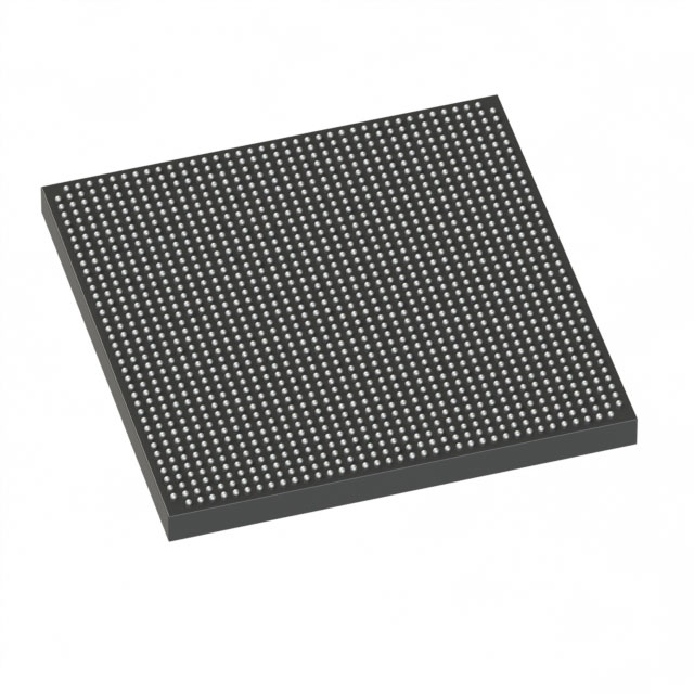
- Package & Mounting 1932‑BBGA, FCBGA package (supplier package listed as 1932‑FBGA, FC (45×45)); surface‑mount mounting type for board‑level integration.
- Temperature Grade Industrial grade with an operating temperature range of −40°C to 100°C for hardened environmental performance.
- RoHS Compliance RoHS‑compliant construction to meet standard lead‑free manufacturing requirements.
- Stratix V GX Family Transceiver Options Stratix V GX devices are offered with GX transceiver speed grades (family documentation lists GX channel options up to 14.1 Gbps), providing options for high‑speed serial connectivity where required.
Typical Applications
- Large-scale logic integration Use the device where substantial programmable logic is needed — 622,000 logic elements enable high gate counts and complex custom architectures.
- Memory‑intensive processing Approximately 51.2 Mbits of embedded RAM supports buffering, packet processing, and on‑chip data handling without external memory for many use cases.
- High‑pin systems and I/O aggregation With 840 I/O pins, deploy the FPGA as a central I/O hub for multi‑lane interfaces and dense board interconnects.
Unique Advantages
- Highly integrated logic and memory: Combines 622,000 logic elements with ~51.2 Mbits of embedded RAM to reduce external component count and simplify system architecture.
- Extensive I/O capacity: 840 I/O pins support dense connectivity, reducing the need for additional interface chips and enabling direct attachment of multiple subsystems.
- Industrial temperature rating: Rated for −40°C to 100°C operation, providing robustness for industrial environments and extended temperature applications.
- High‑density FCBGA package: The 1932‑BBGA/1932‑FBGA (45×45) package provides a compact, high‑pin‑count solution for space‑constrained boards that require large FPGA capacity.
- Family transceiver options: As part of the Stratix V GX family, transceiver speed grades are available for designs that need high‑speed serial channels (family documentation lists GX channel grades up to 14.1 Gbps).
- RoHS compliant: Aligns with lead‑free manufacturing processes and standard environmental requirements.
Why Choose 5SGXMA7N3F45I3WN?
The 5SGXMA7N3F45I3WN positions itself as a high‑capacity Stratix V GX FPGA for applications requiring large programmable logic, substantial embedded memory, and a high number of I/O connections within an industrial temperature envelope. Its combination of 622,000 logic elements, approximately 51.2 Mbits of on‑chip RAM, and 840 I/Os makes it suitable for system designs that prioritize integration and board‑level consolidation.
Supported by Intel’s Stratix V family documentation and supplied in a high‑density 1932 FCBGA package, this device is appropriate for development teams and procurement looking for a robust FPGA platform that aligns with industrial operating conditions and RoHS requirements.
Request a quote or submit an inquiry for part number 5SGXMA7N3F45I3WN to obtain pricing, lead times, and availability for your project requirements.


Date Founded: 1968
Headquarters: Santa Clara, California, USA
Employees: 130,000+
Revenue: $54.23 Billion
Certifications and Memberships: ISO9001:2015, ISO14001:2015, ISO17025:2017, ISO27001:2022, ISO45001:2018, ISO50001:2018


