
5SGXMA9N3F45C2G
| Part Description |
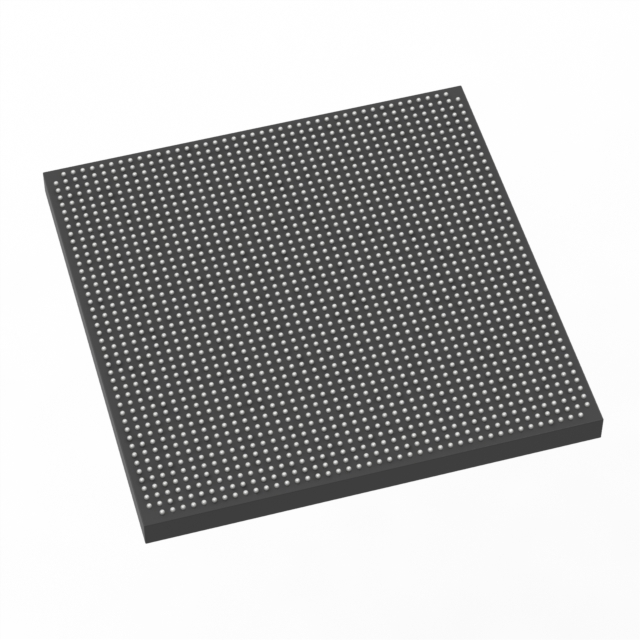
Stratix® V GX Field Programmable Gate Array (FPGA) IC 840 53248000 840000 1932-BBGA, FCBGA |
|---|---|
| Quantity | 325 Available (as of June 18, 2026) |

| Product Category | Field Programmable Gate Array (FPGA) |
|---|---|
| Manufacturer | Intel |
| Manufacturing Status | Active |
| Manufacturer Standard Lead Time | 26 Weeks |
| Datasheet |
Specifications & Environmental
| Device Package | 1932-FBGA, FC (45x45) | Grade | Commercial | Operating Temperature | 0°C – 85°C | ||
|---|---|---|---|---|---|---|---|
| Package / Case | 1932-BBGA, FCBGA | Number of I/O | 840 | Voltage | 870 mV - 930 mV | ||
| Mounting Method | Surface Mount | RoHS Compliance | RoHS Compliant | REACH Compliance | REACH Unaffected | ||
| Moisture Sensitivity Level | 3 (168 Hours) | Number of LABs/CLBs | 317000 | Number of Logic Elements/Cells | 840000 | ||
| Number of Gates | N/A | ECCN | N/A | HTS Code | N/A | ||
| Qualification | N/A | Total RAM Bits | 53248000 |
Overview of 5SGXMA9N3F45C2G – Stratix® V GX Field Programmable Gate Array (FPGA)
The 5SGXMA9N3F45C2G is a high-density Stratix V GX FPGA from Intel, packaged in a 1932-BBGA (FCBGA) format and intended for commercial temperature applications. This device integrates substantial programmable logic, memory, and I/O capacity—including 840,000 logic elements, approximately 53.2 Mbits of embedded memory, and 840 general-purpose I/Os—enabling complex, board-level programmable designs that require large logic and memory resources.
Built on the Stratix V GX family, the device adheres to the family electrical and transceiver characteristics documented in the device datasheet and is supplied as a surface-mount, RoHS-compliant component with a recommended core supply range of 870 mV to 930 mV and an operating temperature range of 0 °C to 85 °C.
Key Features
- Programmable Logic Capacity 840,000 logic elements provide high-density logic resources for complex custom logic and algorithm implementation.
- Embedded Memory Approximately 53.2 Mbits of on-chip RAM to support large buffering, state storage, and data-path acceleration within the fabric.
- High I/O Count 840 I/O pins enable wide parallel interfaces and multiple peripheral connections on a single FPGA.
- Power and Supply Core supply operating range specified at 870 mV to 930 mV to meet the device’s electrical requirements as documented in the datasheet.
- Package and Mounting 1932-BBGA (FCBGA) package, supplier package listed as 1932-FBGA, FC (45×45), and surface-mount mounting for compact board integration.
- Commercial Temperature Grade Rated for commercial operation from 0 °C to 85 °C in accordance with the product data provided.
- Standards and Compliance RoHS-compliant material status for regulatory and manufacturing compatibility.
- Family-Level Transceiver Options As part of the Stratix V GX family, the device is offered across multiple transceiver speed grades per the Stratix V device documentation.
Typical Applications
- High-density custom logic Implement large-scale, application-specific logic and acceleration using the device’s 840,000 logic elements and abundant embedded memory.
- High-port-count I/O systems Support wide parallel interfaces and multiple peripherals with 840 available I/O pins for complex board-level designs.
- Programmable system integration Consolidate multiple functions into a single programmable device using the fabric’s combination of logic, memory, and I/O resources.
Unique Advantages
- Substantial on-chip resources: 840,000 logic elements and approximately 53.2 Mbits of embedded RAM reduce reliance on external logic and memory, simplifying system architecture.
- High I/O density: 840 I/Os provide flexibility for complex interface requirements and multi-channel connectivity without external multiplexing.
- Compact package footprint: 1932-BBGA (FCBGA) package supports high-pin-count designs in a manufacturable surface-mount form factor.
- Commercial-grade availability: Specified for 0 °C to 85 °C operation and RoHS compliance for mainstream electronic product deployment.
- Documented family capabilities: Design and integration can leverage the Stratix V device documentation and electrical characteristics provided in the datasheet.
Why Choose 5SGXMA9N3F45C2G?
This Stratix V GX device is positioned for designs that require a combination of very large programmable logic capacity, significant on-chip memory, and a high number of external I/Os within a commercial temperature envelope. Its surface-mount 1932-BBGA package and RoHS compliance make it suitable for compact, production board-level deployments where consolidation of functions into a single FPGA reduces system complexity.
The device is best suited to engineering teams and procurement organizations seeking a documented, high-density Stratix V GX FPGA with clearly defined electrical parameters (870–930 mV core supply) and commercial operating range (0 °C to 85 °C). Reference to the Stratix V family datasheet is available for detailed electrical and transceiver characteristics when integrating this device into a design.
Request a quote or submit an inquiry to obtain pricing, availability, and additional ordering information for 5SGXMA9N3F45C2G.


Date Founded: 1968
Headquarters: Santa Clara, California, USA
Employees: 130,000+
Revenue: $54.23 Billion
Certifications and Memberships: ISO9001:2015, ISO14001:2015, ISO17025:2017, ISO27001:2022, ISO45001:2018, ISO50001:2018


