
5SGXMABN2F45C2
| Part Description |
Stratix® V GX Field Programmable Gate Array (FPGA) IC 840 53248000 952000 1932-BBGA, FCBGA |
|---|---|
| Quantity | 1,049 Available (as of June 16, 2026) |

| Product Category | Field Programmable Gate Array (FPGA) |
|---|---|
| Manufacturer | Intel |
| Manufacturing Status | Obsolete |
| Manufacturer Standard Lead Time | Contact Us |
| Datasheet |
Specifications & Environmental
| Device Package | 1932-FBGA, FC (45x45) | Grade | Commercial | Operating Temperature | 0°C – 85°C | ||
|---|---|---|---|---|---|---|---|
| Package / Case | 1932-BBGA, FCBGA | Number of I/O | 840 | Voltage | 870 mV - 930 mV | ||
| Mounting Method | Surface Mount | RoHS Compliance | RoHS Compliant | REACH Compliance | REACH Unknown | ||
| Moisture Sensitivity Level | 3 (168 Hours) | Number of LABs/CLBs | 359200 | Number of Logic Elements/Cells | 952000 | ||
| Number of Gates | N/A | ECCN | 3A001A2C | HTS Code | 8542.39.0001 | ||
| Qualification | N/A | Total RAM Bits | 53248000 |
Overview of 5SGXMABN2F45C2 – Stratix V GX FPGA, 952,000 logic elements
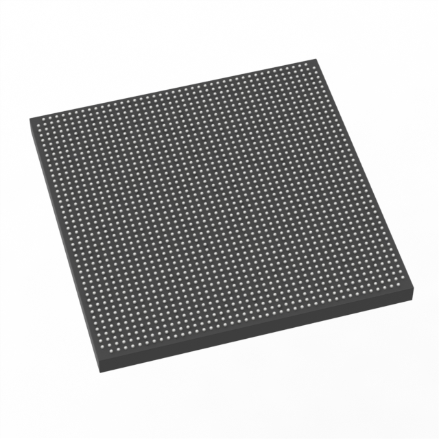
The 5SGXMABN2F45C2 is an Intel Stratix® V GX field programmable gate array (FPGA) packaged in a 1932-ball FCBGA. It delivers very large logic capacity and substantial embedded memory in a single surface-mount device.
With 952,000 logic elements, approximately 53.25 Mbits of embedded memory, and 840 user I/Os, this commercial-grade FPGA supports complex, high-density digital designs that require large on‑chip resources and high I/O capacity.
Key Features
- Core Logic 952,000 logic elements for implementing large-scale digital logic and complex algorithms.
- Logic Array Blocks 359,200 logic array blocks (LABs) for structured logic partitioning and design organization.
- Embedded Memory Approximately 53.25 Mbits of on-chip RAM to support buffering, lookup tables, and data processing without external memory.
- I/O Capacity 840 user I/O pins to support wide parallel interfaces, multiple high-pin-count peripherals, and dense board-level connectivity.
- Power Core supply range from 870 mV to 930 mV to match system power-rail designs and enable predictable core power behavior.
- Package & Mounting 1932-ball BGA (FCBGA) package in a 45 × 45 mm footprint; surface-mount mounting for modern PCB assembly.
- Operating Range & Grade Commercial temperature grade with an operating range of 0 °C to 85 °C.
- Environmental Compliance RoHS compliant to meet common environmental and safety requirements.
Typical Applications
- High-density digital processing — Implement large-scale combinational and sequential logic for signal processing and algorithm acceleration using extensive logic and embedded RAM.
- Board-level integration with high I/O counts — Support complex multi-interface systems and parallel data paths with 840 user I/Os.
- Prototyping and system validation — Use the device’s large resource pool to validate large hardware designs and integrations on a single FPGA.
Unique Advantages
- High logic density: 952,000 logic elements provide the capacity to implement complex, large-scale designs without partitioning across multiple devices.
- Substantial on-chip memory: Approximately 53.25 Mbits of embedded RAM reduces dependency on external memory and improves data throughput and latency.
- Extensive I/O capability: 840 I/Os enable broad peripheral support, wide buses, and flexible board-level routing for multi-interface systems.
- Compact, assembly-ready package: 1932-ball FCBGA (45×45 mm) offers dense integration with surface-mount assembly for modern PCBs.
- Predictable power domain: Defined core supply range (870–930 mV) helps integrate the device into controlled power architectures.
- Commercial-grade operation: Rated for 0 °C to 85 °C, suitable for a wide range of non-industrial applications where commercial temperature range is appropriate.
Why Choose 5SGXMABN2F45C2?
The 5SGXMABN2F45C2 combines very large logic capacity, significant on-chip memory, and extensive I/O in a single Stratix V GX FCBGA package, delivering an integrated platform for complex digital implementations. Its commercial operating range and clearly defined power requirements make it suitable for designers who need high resource density and predictable electrical characteristics.
This device is appropriate for teams developing large FPGA-based systems that benefit from consolidating logic and memory on-chip, reducing external components and simplifying board-level design while relying on Intel’s Stratix V family documentation for electrical and switching characteristics.
Request a quote or submit a purchase inquiry for the 5SGXMABN2F45C2 to discuss availability and pricing.


Date Founded: 1968
Headquarters: Santa Clara, California, USA
Employees: 130,000+
Revenue: $54.23 Billion
Certifications and Memberships: ISO9001:2015, ISO14001:2015, ISO17025:2017, ISO27001:2022, ISO45001:2018, ISO50001:2018


