
5SGXMABN2F45I2LNCV
| Part Description |
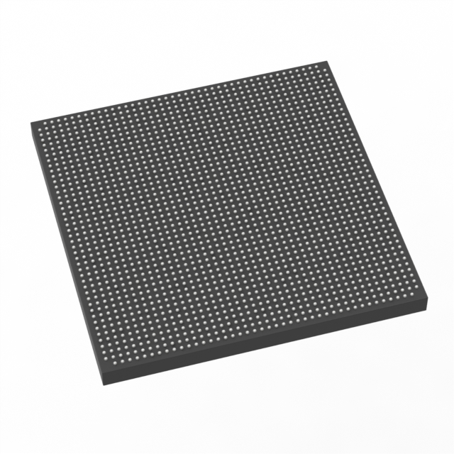
Stratix® V GX Field Programmable Gate Array (FPGA) IC 840 53248000 952000 1932-BBGA, FCBGA |
|---|---|
| Quantity | 285 Available (as of June 14, 2026) |

| Product Category | Field Programmable Gate Array (FPGA) |
|---|---|
| Manufacturer | Intel |
| Manufacturing Status | Obsolete |
| Manufacturer Standard Lead Time | Contact Us |
| Datasheet |
Specifications & Environmental
| Device Package | 1932-FBGA, FC (45x45) | Grade | Industrial | Operating Temperature | -40°C – 100°C | ||
|---|---|---|---|---|---|---|---|
| Package / Case | 1932-BBGA, FCBGA | Number of I/O | 840 | Voltage | 820 mV - 880 mV | ||
| Mounting Method | Surface Mount | RoHS Compliance | RoHS non-compliant | REACH Compliance | REACH Unknown | ||
| Moisture Sensitivity Level | 4 (72 Hours) | Number of LABs/CLBs | 359200 | Number of Logic Elements/Cells | 952000 | ||
| Number of Gates | N/A | ECCN | OBSOLETE | HTS Code | N/A | ||
| Qualification | N/A | Total RAM Bits | 53248000 |
Overview of 5SGXMABN2F45I2LNCV – Stratix® V GX FPGA, 1932-BBGA FCBGA
The 5SGXMABN2F45I2LNCV is an Intel Stratix® V GX field programmable gate array (FPGA) in a 1932-ball FCBGA package. It delivers a high-density programmable logic fabric paired with substantial embedded memory and a large I/O count for complex, high-throughput digital designs.
Targeted at industrial temperature applications, this device provides a combination of logic capacity, on-chip RAM, and low-voltage core operation that supports compute-intensive and high-bandwidth system functions where reliability across –40 °C to 100 °C is required.
Key Features
- High-density logic — 952,000 logic elements to implement large-scale digital designs and complex system functions.
- Significant embedded memory — Approximately 53 Mbits of on-chip RAM to support buffering, packet processing, and DSP workloads.
- Extensive I/O — 840 I/Os to enable broad interfacing with high-pin-count systems and multi-channel designs.
- Industrial temperature grade — Rated for operation from –40 °C to 100 °C for use in industrial environments.
- Low-voltage core — Core voltage supply range of 820 mV to 880 mV for compatibility with low-voltage system architectures.
- Robust package options — 1932-BBGA (FCBGA) surface-mount package; supplier device package listed as 1932-FBGA, FC (45×45).
- Surface-mount mounting — Designed for modern PCB assembly processes with surface-mount package.
- RoHS compliant — Meets RoHS environmental requirements.
Typical Applications
- High-speed networking and communications — Large logic capacity and abundant I/O make this FPGA suitable for packet processing, protocol bridging, and data-plane acceleration.
- Data-center acceleration — On-chip memory and dense logic enable implementation of hardware accelerators and custom compute kernels.
- Telecommunications infrastructure — Industrial temperature rating and high I/O count support ruggedized telecom line cards and baseband processing modules.
- High-performance embedded systems — Use in complex control, signal processing, or multi-interface embedded platforms requiring substantial programmable resources.
Unique Advantages
- High-density programmable fabric: 952,000 logic elements provide the capacity for large custom hardware designs without external logic expansion.
- Large embedded memory: Approximately 53 Mbits of on-chip RAM reduces reliance on external memory for buffering and stateful processing.
- Wide I/O availability: 840 I/Os enable direct connectivity to a broad range of peripherals, transceivers, and parallel interfaces.
- Industrial temperature support: Rated operation from –40 °C to 100 °C for deployment in industrial environments.
- Low-voltage core operation: 820–880 mV core supply supports integration into low-voltage power domains.
- Production-ready package: 1932-BBGA FCBGA surface-mount package supports high-density board-level integration.
Why Choose 5SGXMABN2F45I2LNCV?
This Intel Stratix V GX FPGA combines very high logic density, substantial embedded memory, and expansive I/O in a single industrial-grade FCBGA package. It is positioned for system designs that require scalable programmable compute, extensive interfacing, and reliable operation across a broad temperature range.
Designers building high-throughput networking, communication infrastructure, or compute-accelerated embedded systems will find the device’s capacity and package options conducive to integration, while RoHS compliance and surface-mount packaging support modern manufacturing workflows.
Request a quote or submit a pricing request to evaluate the 5SGXMABN2F45I2LNCV for your next high-density FPGA design.


Date Founded: 1968
Headquarters: Santa Clara, California, USA
Employees: 130,000+
Revenue: $54.23 Billion
Certifications and Memberships: ISO9001:2015, ISO14001:2015, ISO17025:2017, ISO27001:2022, ISO45001:2018, ISO50001:2018


