
5SGXMB5R3F43C2G
| Part Description |
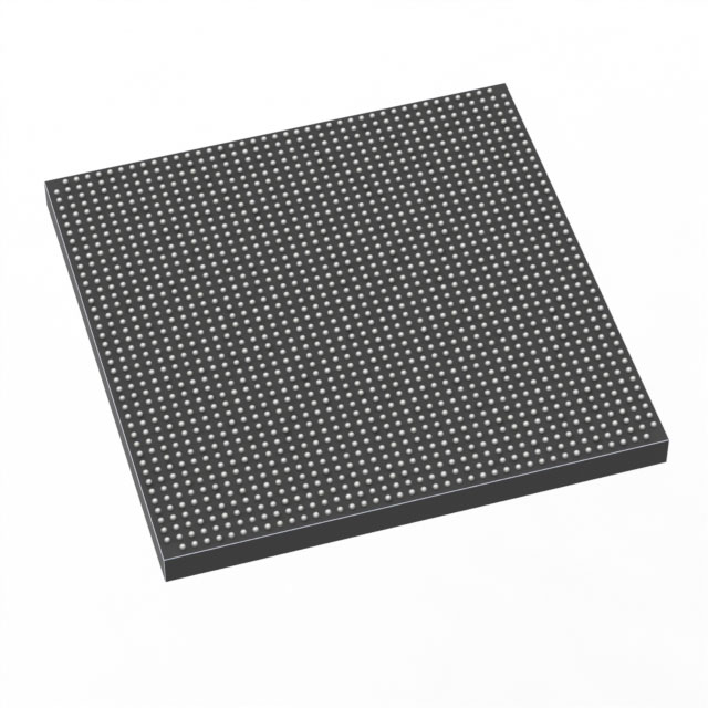
Stratix® V GX Field Programmable Gate Array (FPGA) IC 600 41984000 490000 1760-BBGA, FCBGA |
|---|---|
| Quantity | 797 Available (as of June 15, 2026) |

| Product Category | Field Programmable Gate Array (FPGA) |
|---|---|
| Manufacturer | Intel |
| Manufacturing Status | Active |
| Manufacturer Standard Lead Time | 26 Weeks |
| Datasheet |
Specifications & Environmental
| Device Package | 1760-FCBGA (42.5x42.5) | Grade | Commercial | Operating Temperature | 0°C – 85°C | ||
|---|---|---|---|---|---|---|---|
| Package / Case | 1760-BBGA, FCBGA | Number of I/O | 600 | Voltage | 870 mV - 930 mV | ||
| Mounting Method | Surface Mount | RoHS Compliance | RoHS Compliant | REACH Compliance | REACH Unaffected | ||
| Moisture Sensitivity Level | 3 (168 Hours) | Number of LABs/CLBs | 185000 | Number of Logic Elements/Cells | 490000 | ||
| Number of Gates | N/A | ECCN | N/A | HTS Code | N/A | ||
| Qualification | N/A | Total RAM Bits | 41984000 |
Overview of 5SGXMB5R3F43C2G – Stratix® V GX Field Programmable Gate Array (FPGA)
The 5SGXMB5R3F43C2G is a Stratix V GX family FPGA from Intel, offered in a 1760-FCBGA (42.5×42.5) surface-mount package for commercial-temperature applications. It provides a high-density programmable logic fabric paired with significant on-chip memory and a large I/O count for complex, high-performance designs.
Designed as part of the Stratix V GX series, this device is characterized in the series datasheet for core and periphery switching characteristics and for multi-gigabit transceiver capabilities. The combination of dense logic, embedded RAM, and extensive I/O makes it suitable for designs that require substantial on-chip resources and high-speed connectivity within a commercial temperature range.
Key Features
- Logic Capacity Approximately 490,000 logic elements for large-scale programmable logic implementations.
- Embedded Memory Approximately 42 Mbits of embedded memory (41,984,000 total RAM bits) to support large buffering, lookup tables, and data storage on-chip.
- I/O Resources Up to 600 I/O pins to interface with high-pin-count systems and multiple external peripherals.
- Power Supply Core voltage supply range specified at 870 mV to 930 mV for operation within the device’s electrical requirements.
- Package & Mounting 1760-FCBGA (42.5×42.5 mm) ball-grid array, surface-mount mounting for dense PCB integration.
- Commercial Grade Temperature Rated for operation from 0 °C to 85 °C, suitable for commercial-environment electronics.
- RoHS Compliant Manufactured to meet RoHS environmental standards.
- Stratix V GX Family Characteristics Series-level electrical and switching characteristics, including transceiver specifications, are documented in the Stratix V device datasheet.
Typical Applications
- High-speed serial systems Leverage the Stratix V GX family’s transceiver-focused design for multi-gigabit serial links and high-bandwidth data transport.
- Custom acceleration and compute Dense logic and substantial on-chip RAM enable custom processing engines and hardware accelerators within commercial systems.
- Telecommunications and networking Large I/O count and on-chip resources support packet processing, aggregation, and protocol interfaces in commercial networking equipment.
- Prototyping and complex system integration High logic element count and extensive I/O make the device suitable for prototype platforms and integrated system designs that consolidate multiple functions on a single FPGA.
Unique Advantages
- High-density programmable fabric: The device’s ~490,000 logic elements provide the capacity to implement complex state machines, datapaths, and custom logic without extensive external ASIC resources.
- Significant embedded memory: Approximately 42 Mbits of on-chip RAM reduces reliance on external memory for buffering and LUT-based functions, improving system integration.
- Large I/O complement: 600 I/O pins allow flexible interfacing to peripherals, mezzanine cards, and high-pin-count connectors common in commercial systems.
- Commercial temperature rating: Rated 0 °C to 85 °C for deployment in standard commercial environments where rugged industrial grades are not required.
- Compact FCBGA packaging: The 1760-FCBGA (42.5×42.5) package supports high-density PCB layouts while maintaining a surface-mount form factor for automated assembly.
- Standards-conscious manufacturing: RoHS compliance supports environmentally regulated product designs.
Why Choose 5SGXMB5R3F43C2G?
The 5SGXMB5R3F43C2G combines the Stratix V GX family’s series-level transceiver and switching characteristics with a high logic element count, substantial embedded memory, and a large I/O complement—delivering a commercially rated FPGA platform for advanced system designs. Its 1760-FCBGA surface-mount package and specified core voltage range are suitable for dense, performance-oriented boards in commercial applications.
This device is well suited for engineering teams building high-performance networking, compute acceleration, or multi-interface systems who need a highly integrated FPGA with significant on-chip resources and documented electrical and switching behavior within the Stratix V datasheet.
If you would like pricing, availability, or to request a quote for 5SGXMB5R3F43C2G, please submit a quote request or inquiry and our team will respond with the next steps.


Date Founded: 1968
Headquarters: Santa Clara, California, USA
Employees: 130,000+
Revenue: $54.23 Billion
Certifications and Memberships: ISO9001:2015, ISO14001:2015, ISO17025:2017, ISO27001:2022, ISO45001:2018, ISO50001:2018


