
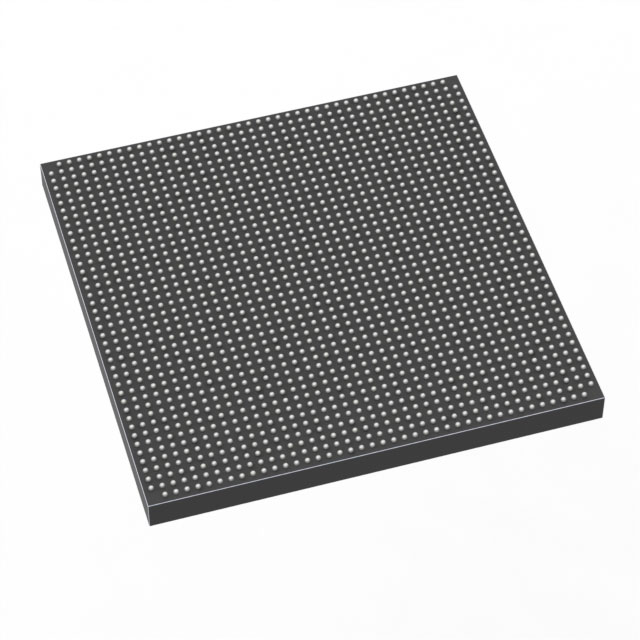
5SGXMB5R3F43C3G
| Part Description |
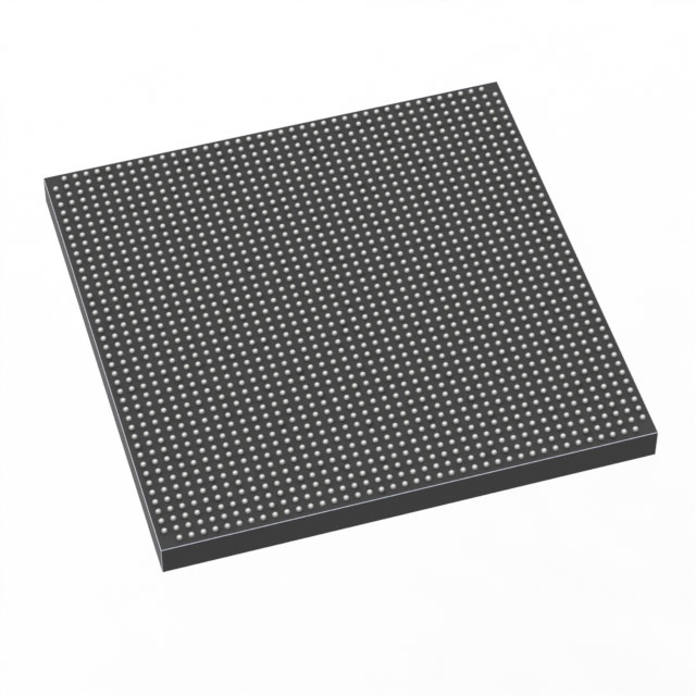
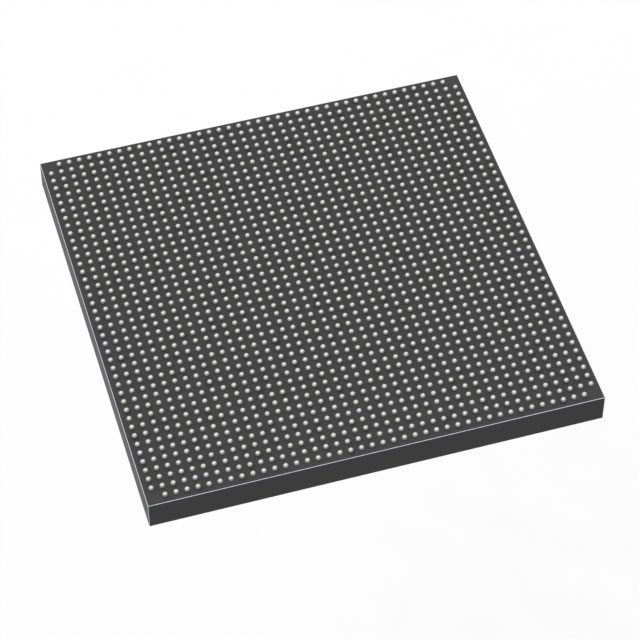
Stratix® V GX Field Programmable Gate Array (FPGA) IC 600 41984000 490000 1760-BBGA, FCBGA |
|---|---|
| Quantity | 250 Available (as of October 8, 2026) |
| Product Category | Field Programmable Gate Array (FPGA) |
|---|---|
| Manufacturer | Intel |
| Manufacturing Status | Active |
| Manufacturer Standard Lead Time | 26 Weeks |
| Datasheet |
Specifications & Environmental
| Device Package | 1760-FCBGA (42.5x42.5) | Grade | Commercial | Operating Temperature | 0°C – 85°C | ||
|---|---|---|---|---|---|---|---|
| Package / Case | 1760-BBGA, FCBGA | Number of I/O | 600 | Voltage | 820 mV - 880 mV | ||
| Mounting Method | Surface Mount | RoHS Compliance | RoHS Compliant | REACH Compliance | REACH Unaffected | ||
| Moisture Sensitivity Level | 3 (168 Hours) | Number of LABs/CLBs | 185000 | Number of Logic Elements/Cells | 490000 | ||
| Number of Gates | N/A | ECCN | N/A | HTS Code | N/A | ||
| Qualification | N/A | Total RAM Bits | 41984000 |
Overview of 5SGXMB5R3F43C3G – Stratix® V GX Field Programmable Gate Array (FPGA) IC
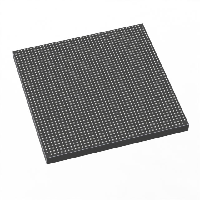
The 5SGXMB5R3F43C3G is a Stratix V GX family FPGA in a 1760-FCBGA package, designed for high-density programmable logic and extensive I/O integration. This commercial-grade device combines a large logic fabric, substantial on-chip RAM, and a broad transceiver capability defined by the Stratix V GX device family specifications.
Key attributes include approximately 490,000 logic elements, roughly 42 Mbits of embedded memory, and 600 user I/O pins, making this device suitable for complex, I/O-intensive designs that require high logic capacity and configurable high-speed serial interfaces.
Key Features
- Core logic Approximately 490,000 logic elements for implementing large-scale digital logic and custom processing pipelines.
- Embedded memory Approximately 42 Mbits of on-chip RAM to support wide buffering, look-up tables, and state storage.
- High-density I/O 600 user I/O pins to accommodate extensive peripheral connectivity and multi-channel interfacing.
- Transceiver capability (Stratix V GX family) Stratix V GX devices include high-speed transceiver grades (GX channel speeds listed in the device datasheet up to 14.1 Gbps for certain grades), providing options for high-rate serial links where required.
- Power and operating conditions Core voltage supply range of 820 mV to 880 mV and commercial operating temperature range of 0 °C to 85 °C.
- Package and mounting 1760-FCBGA package (42.5 × 42.5 mm) in a surface-mount form factor for board-level integration.
- Compliance RoHS-compliant to support environmentally conscious manufacturing and assembly.
Typical Applications
- High-speed serial interfaces Leverage the Stratix V GX device family transceiver grades for systems that require multi-gigabit serial links.
- Large-scale programmable logic Use the substantial logic element count and embedded memory for complex digital processing, protocol implementation, and algorithm acceleration.
- Dense I/O aggregation Support systems requiring many external sensors, ADCs/DACs, or parallel interfaces using the device’s 600 I/O pins.
Unique Advantages
- High integration density: Nearly half a million logic elements reduce the need for multiple devices when implementing complex designs.
- Large on-chip memory: Approximately 42 Mbits of embedded RAM simplifies buffering and state storage without relying on external memory.
- Extensive I/O capability: 600 user I/Os enable broad peripheral connectivity and flexible system partitioning.
- Commercial-grade operating range: Defined 0 °C to 85 °C operating temperature and specified core supply range allow predictable integration into commercial products.
- Industry-standard package: 1760-FCBGA (42.5 × 42.5 mm) surface-mount package supports high-density PCB layouts and established assembly processes.
Why Choose 5SGXMB5R3F43C3G?
The 5SGXMB5R3F43C3G delivers a combination of large logic capacity, considerable embedded memory, and extensive I/O in a single commercial-grade Stratix V GX FPGA. It is appropriate for designers who need to consolidate complex logic, implement wide buffering, and support numerous external interfaces while retaining the configurability of an FPGA.
For projects requiring scalable logic resources and configurable high-speed serial capabilities defined by the Stratix V GX family, this device offers a clear specification set—dense logic, substantial on-chip RAM, multi-hundred I/O count, RoHS compliance, and a defined commercial operating window—backed by the Stratix V device documentation.
Request a quote or submit an inquiry to discuss availability, lead time, and pricing for the 5SGXMB5R3F43C3G. Our team can provide ordering information and technical documentation to support your design evaluation.





















Date Founded: 1968
Headquarters: Santa Clara, California, USA
Employees: 130,000+
Revenue: $54.23 Billion
Certifications and Memberships: ISO9001:2015, ISO14001:2015, ISO17025:2017, ISO27001:2022, ISO45001:2018, ISO50001:2018


