
5SGXMB9R3H43C2LG
| Part Description |
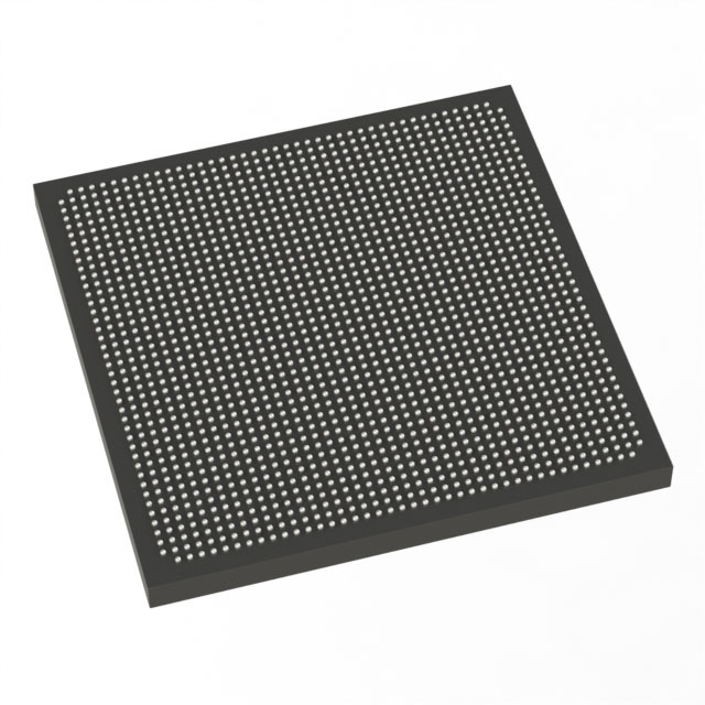
Stratix® V GX Field Programmable Gate Array (FPGA) IC 600 53248000 840000 1760-BBGA, FCBGA |
|---|---|
| Quantity | 752 Available (as of June 15, 2026) |

| Product Category | Field Programmable Gate Array (FPGA) |
|---|---|
| Manufacturer | Intel |
| Manufacturing Status | Active |
| Manufacturer Standard Lead Time | 26 Weeks |
| Datasheet |
Specifications & Environmental
| Device Package | 1760-HBGA (45x45) | Grade | Commercial | Operating Temperature | 0°C – 85°C | ||
|---|---|---|---|---|---|---|---|
| Package / Case | 1760-BBGA, FCBGA | Number of I/O | 600 | Voltage | 820 mV - 880 mV | ||
| Mounting Method | Surface Mount | RoHS Compliance | RoHS Compliant | REACH Compliance | REACH Unaffected | ||
| Moisture Sensitivity Level | 3 (168 Hours) | Number of LABs/CLBs | 317000 | Number of Logic Elements/Cells | 840000 | ||
| Number of Gates | N/A | ECCN | N/A | HTS Code | N/A | ||
| Qualification | N/A | Total RAM Bits | 53248000 |
Overview of 5SGXMB9R3H43C2LG – Stratix® V GX FPGA, 1760-BBGA FCBGA, 600 I/Os
The 5SGXMB9R3H43C2LG is a Stratix V GX Field Programmable Gate Array (FPGA) IC designed for high-density logic and embedded memory applications. It combines a large logic fabric, substantial on-chip RAM, and a broad I/O count in a 1760-BBGA (FCBGA) package for integration into complex digital systems.
Targeted at commercial-temperature applications, this device is suited for designs that require significant programmable logic capacity, wide I/O connectivity, and support for Stratix V GX transceiver speed grades as documented in the device datasheet.
Key Features
- Core & Logic — 840,000 logic elements provide extensive programmable logic capacity for complex algorithms and large-scale state machines.
- Logic Array Blocks — 317,000 logic array blocks (LABs/CLBs reported in device data) for structured logic partitioning and resource planning.
- Embedded Memory — Approximately 53 Mbits of on-chip RAM to support buffering, DSP data storage, and large LUTRAM implementations.
- I/O Density — 600 available I/O pins to accommodate wide parallel interfaces, multiple peripheral buses, or extensive board-level connectivity.
- High-speed Transceivers — Stratix V GX transceiver speed grades are documented in the datasheet (GX channel listings include speeds up to 14.1 Gbps), enabling high-bandwidth serial links where required.
- Power & Supply — Core supply voltage range from 820 mV to 880 mV for planning power delivery and regulator selection.
- Package & Mounting — 1760-BBGA, FCBGA package (supplier package listed as 1760-HBGA, 45 × 45 mm) for surface-mount PCB integration with high I/O density.
- Operating Range — Commercial temperature grade with an operating range of 0 °C to 85 °C.
- Regulatory Compliance — RoHS compliant.
Typical Applications
- High-density signal processing — Use the large pool of logic elements and abundant on-chip RAM for DSP pipelines, video processing, and real-time data manipulation.
- Network and communications equipment — Leverage the Stratix V GX transceiver speed grades and 600 I/Os for high-bandwidth serial links, protocol bridging, and packet processing.
- Prototyping and complex SoC integration — Implement custom accelerators, bus fabrics, and system glue logic with the device’s extensive logic and memory resources.
Unique Advantages
- Large programmable fabric: 840,000 logic elements enable consolidation of multi-module designs into a single FPGA, reducing external components.
- Substantial embedded memory: Approximately 53 Mbits of on-chip RAM minimizes external memory dependence and improves system latency.
- High I/O count: 600 I/Os give flexibility to connect multiple parallel interfaces or mix high-speed serial and parallel peripherals on one device.
- Documented transceiver capability: GX transceiver speed grades are specified in the Stratix V datasheet, supporting high-bandwidth link designs when required.
- Commercial temperature operation: Rated 0 °C to 85 °C for standard commercial deployments and system integration planning.
- RoHS compliant: Meets common environmental compliance requirements for modern electronics manufacturing.
Why Choose 5SGXMB9R3H43C2LG?
The 5SGXMB9R3H43C2LG offers a combination of expansive logic resources, significant embedded memory, and high I/O density in a single Stratix V GX device. Its specifications make it a practical option for engineers designing complex digital systems that require on-chip capacity for logic, buffering, and high-bandwidth I/O.
Backed by the Stratix V device documentation, this part is appropriate for commercial-temperature deployments where deterministic FPGA resources and documented transceiver speed grades are required. It provides a scalable platform for integrating compute-heavy or I/O-intensive functions while simplifying board-level architecture.
Request a quote or submit a procurement inquiry to obtain pricing, lead time, and availability for the 5SGXMB9R3H43C2LG.


Date Founded: 1968
Headquarters: Santa Clara, California, USA
Employees: 130,000+
Revenue: $54.23 Billion
Certifications and Memberships: ISO9001:2015, ISO14001:2015, ISO17025:2017, ISO27001:2022, ISO45001:2018, ISO50001:2018


