
A3P1000-2FGG256
| Part Description |
ProASIC3 Field Programmable Gate Array (FPGA) IC 177 147456 256-LBGA |
|---|---|
| Quantity | 744 Available (as of June 15, 2026) |
| Product Category | Field Programmable Gate Array (FPGA) |
|---|---|
| Manufacturer | Microchip Technology |
| Manufacturing Status | Active |
| Manufacturer Standard Lead Time | 10 Weeks |
| Datasheet |
Specifications & Environmental
| Device Package | 256-FPBGA (17x17) | Grade | Commercial | Operating Temperature | 0°C – 85°C | ||
|---|---|---|---|---|---|---|---|
| Package / Case | 256-LBGA | Number of I/O | 177 | Voltage | 1.425 V - 1.575 V | ||
| Mounting Method | Surface Mount | RoHS Compliance | ROHS3 Compliant | REACH Compliance | REACH Unaffected | ||
| Moisture Sensitivity Level | 3 (168 Hours) | Number of LABs/CLBs | 24576 | Number of Logic Elements/Cells | 24576 | ||
| Number of Gates | 1000000 | ECCN | 3A991D | HTS Code | 8542.39.0001 | ||
| Qualification | N/A | Total RAM Bits | 147456 |
Overview of A3P1000-2FGG256 – ProASIC3 Field Programmable Gate Array, 256-LBGA
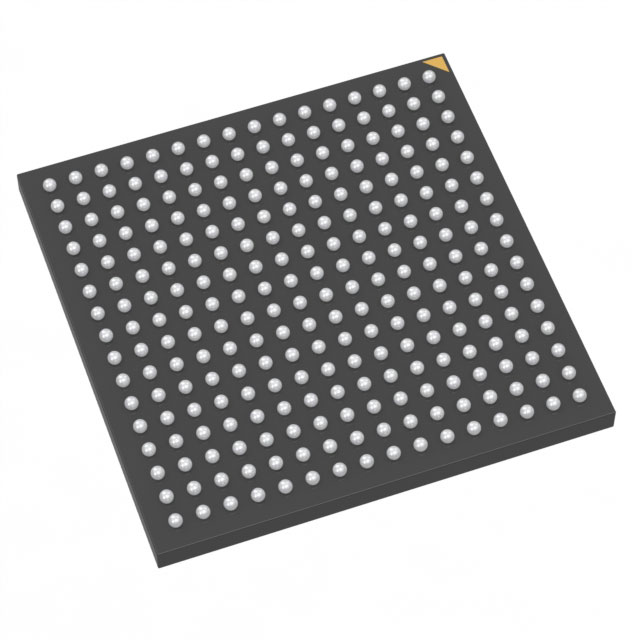
The A3P1000-2FGG256 is a ProASIC3 field programmable gate array (FPGA) from Microchip Technology, packaged in a 256-LBGA surface-mount package. It delivers a high-capacity combination of logic, I/O, and on-chip memory for commercial embedded and digital logic applications.
With 24,576 logic elements (approximately 1,000,000 gates), 177 I/O pins, and roughly 0.15 Mbits of embedded RAM, this device targets designs that require substantial logic density and high I/O count within a compact 256-LBGA footprint. The device operates from a 1.425 V to 1.575 V supply and is specified for commercial temperature use (0 °C to 85 °C).
Key Features
- Core Logic 24,576 logic elements providing a total of 1,000,000 gates to implement complex digital functions and custom datapaths.
- Embedded Memory Approximately 0.15 Mbits of on-chip RAM (147,456 bits) for local buffering, small lookup tables, and state storage.
- I/O Capacity 177 user I/O pins suitable for dense interface and connectivity requirements.
- Power Defined supply range of 1.425 V to 1.575 V for core power planning and system integration.
- Package and Mounting 256-LBGA package (supplier package: 256-FPBGA, 17×17) in a surface-mount form factor for compact board layouts.
- Operating Range Commercial grade device rated for operation from 0 °C to 85 °C.
- Environmental Compliance RoHS compliant to support environmental material requirements.
Typical Applications
- Custom Digital Logic and Control Implement state machines, timing-critical control logic, and custom datapaths using the device’s 24,576 logic elements and 1,000,000 gates.
- Interface Bridging and I/O Consolidation Consolidate multiple interfaces or provide dense connectivity using up to 177 I/O pins to reduce external glue logic.
- Embedded System Gateware Use on-chip RAM (approximately 0.15 Mbits) with internal logic resources for local buffering, lookup tables, and embedded control functions.
- Space-Constrained Board Designs Leverage the 256-LBGA (17×17) surface-mount package to integrate high logic density in compact PCB layouts.
Unique Advantages
- High logic density: 24,576 logic elements and 1,000,000 gates deliver substantial capacity for mid-to-high complexity digital designs.
- Ample I/O connectivity: 177 I/O pins reduce the need for external multiplexers and simplify system-level routing.
- On-chip memory: Approximately 0.15 Mbits of embedded RAM supports local data storage and reduces dependence on external memory for small buffers.
- Compact LBGA package: 256-LBGA (256-FPBGA, 17×17) balances I/O count and package density for modern PCB constraints.
- Clear electrical and thermal envelope: Defined supply range (1.425 V–1.575 V) and commercial temperature rating (0 °C–85 °C) simplify system integration and validation.
- RoHS compliant: Meets environmental material restrictions for streamlined regulatory adherence.
Why Choose A3P1000-2FGG256?
The A3P1000-2FGG256 positions itself as a compact, commercially rated FPGA that combines significant logic capacity, substantial I/O, and on-chip memory within a 256-LBGA footprint. It is well suited for engineers and procurement teams working on embedded systems, interface consolidation, and medium-to-high complexity digital designs that require a defined power and temperature envelope.
Produced by Microchip Technology, this device offers a balance of integration and board-level density for customers seeking a surface-mount FPGA solution with clear, verifiable specifications for logic, memory, I/O, supply voltage, and operating temperature.
Request a quote or submit a request for pricing and availability for the A3P1000-2FGG256 to get detailed commercial terms and lead-time information.


Date Founded: 1989
Headquarters: Chandler, Arizona, USA
Employees: 22,000+
Revenue: $8.349 Billion
Certifications and Memberships: ISO9001:2015, IATF16949:2016, AS 9100D


