
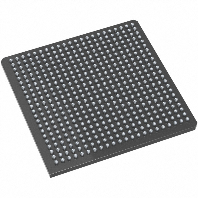
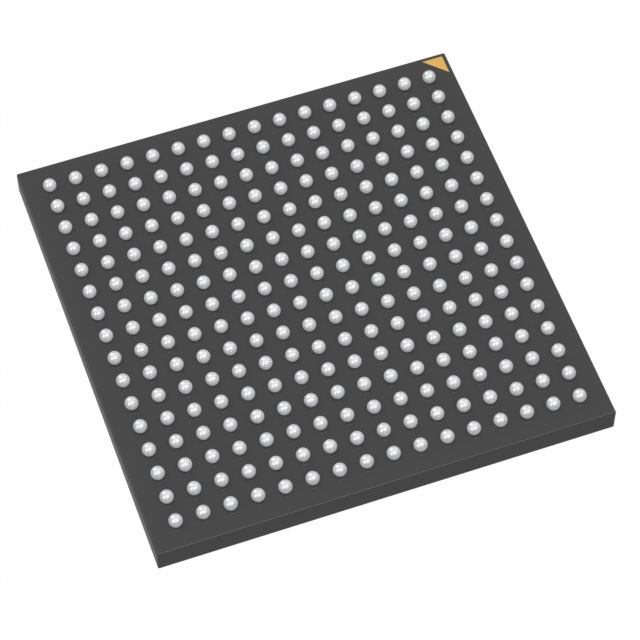
A3P1000-FGG144T
| Part Description |
ProASIC3 Field Programmable Gate Array (FPGA) IC 97 147456 144-LBGA |
|---|---|
| Quantity | 474 Available (as of June 15, 2026) |

| Product Category | Field Programmable Gate Array (FPGA) |
|---|---|
| Manufacturer | Microchip Technology |
| Manufacturing Status | Active |
| Manufacturer Standard Lead Time | 18 Weeks |
| Datasheet |
Specifications & Environmental
| Device Package | 144-FPBGA (13x13) | Grade | Automotive | Operating Temperature | -40°C – 125°C | ||
|---|---|---|---|---|---|---|---|
| Package / Case | 144-LBGA | Number of I/O | 97 | Voltage | 1.425 V - 1.575 V | ||
| Mounting Method | Surface Mount | RoHS Compliance | ROHS3 Compliant | REACH Compliance | REACH Unaffected | ||
| Moisture Sensitivity Level | 3 (168 Hours) | Number of LABs/CLBs | 24576 | Number of Logic Elements/Cells | 24576 | ||
| Number of Gates | 1000000 | ECCN | 3A991D | HTS Code | 8542.39.0001 | ||
| Qualification | AEC-Q100 | Total RAM Bits | 147456 |
Overview of A3P1000-FGG144T – ProASIC3 FPGA, 97 I/O, 144-LBGA
The A3P1000-FGG144T is a ProASIC3 field programmable gate array (FPGA) from Microchip Technology designed for robust embedded logic integration. It provides 24,576 logic elements and approximately 0.15 Mbits of on-chip RAM in a compact 144-LBGA package, targeting applications that require programmable logic, deterministic operation, and broad I/O connectivity.
With an operating temperature range from -40 °C to 125 °C and AEC-Q100 qualification, this device addresses automotive-grade deployment requirements while offering a dense logic fabric and flexible I/O resources for control, interface, and signal-processing tasks.
Key Features
- Logic Capacity 24,576 logic elements (logic cells) providing substantial programmable fabric for glue logic, state machines, and custom IP integration.
- On-chip Memory Approximately 0.15 Mbits (147,456 bits) of embedded RAM to support buffering, small data structures, and on-chip scratch memory for algorithms.
- Gate Count Approximately 1,000,000 gates for mapping complex logic and interconnect structures within the FPGA.
- I/O Resources 97 general-purpose I/O pins to connect sensors, actuators, and peripheral interfaces directly to the FPGA fabric.
- Package and Mounting 144-LBGA package (supplier package 144-FPBGA, 13×13) in a surface-mount form factor for compact board layouts.
- Power Specified core supply range of 1.425 V to 1.575 V to match system power rails and enable consistent device operation.
- Automotive Qualification AEC-Q100 qualification and an operating temperature range of -40 °C to 125 °C, meeting automotive-grade environmental requirements.
- Compliance RoHS-compliant component suitable for modern electronics manufacturing practices.
Typical Applications
- Automotive electronics Use in engine, body, or chassis control modules where AEC-Q100 qualification and extended temperature range are required for reliable operation.
- Sensor interfaces Aggregate and preprocess sensor signals using on-chip logic and RAM to reduce system latency and offload microcontroller resources.
- Control and actuation Implement deterministic control logic, state machines, and I/O handling for motor drivers, valve control, and other embedded control functions.
- Protocol bridging Customize interface logic to bridge or adapt between disparate serial or parallel interfaces using available I/O and programmable logic resources.
Unique Advantages
- Automotive-qualified design: AEC-Q100 qualification and -40 °C to 125 °C operating range enable deployment in automotive environments where temperature and reliability matter.
- High logic density: 24,576 logic elements and ~1,000,000 gates allow consolidation of multiple discrete functions into a single FPGA, reducing bill-of-materials and board complexity.
- Integrated on-chip memory: 147,456 bits of embedded RAM provide local storage for buffering and temporary data without external memory components.
- Ample I/O count: 97 I/O pins deliver flexible connectivity for sensors, actuators, and peripheral devices, simplifying system integration.
- Compact surface-mount package: 144-LBGA (13×13 FPBGA) supports space-constrained PCB designs while maintaining robust soldered connections.
- Tightly specified supply range: Defined core voltage range (1.425 V–1.575 V) helps designers align power delivery for predictable device behavior.
Why Choose A3P1000-FGG144T?
The A3P1000-FGG144T combines substantial programmable logic capacity, on-chip RAM, and a generous I/O complement in an automotive-qualified package. It is well suited to engineers building automotive control, sensor interface, and protocol-bridging solutions that require deterministic, on-board programmable logic operating across extended temperature conditions.
As part of the ProASIC3 family from Microchip Technology, this device offers a blend of integration and reliability for projects that need a compact, automotive-grade FPGA with clear electrical and environmental specifications.
Request a quote or submit an inquiry for the A3P1000-FGG144T to discuss pricing, lead times, and availability for your design.


Date Founded: 1989
Headquarters: Chandler, Arizona, USA
Employees: 22,000+
Revenue: $8.349 Billion
Certifications and Memberships: ISO9001:2015, IATF16949:2016, AS 9100D


