
A3P250-FGG144I
| Part Description |
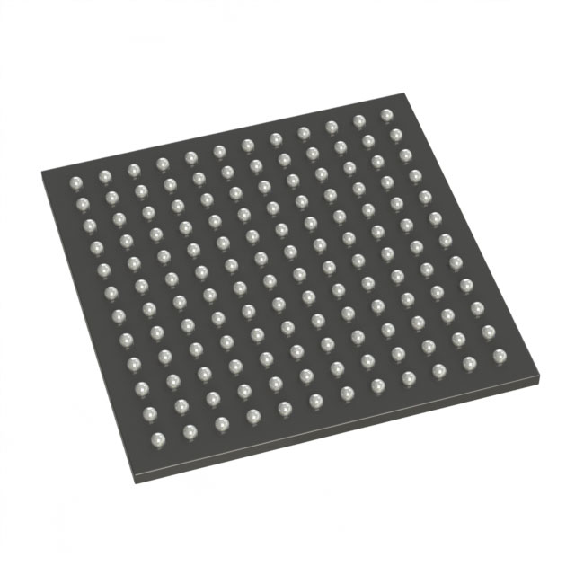
ProASIC3 Field Programmable Gate Array (FPGA) IC 97 36864 144-LBGA |
|---|---|
| Quantity | 289 Available (as of October 7, 2026) |
| Product Category | Field Programmable Gate Array (FPGA) |
|---|---|
| Manufacturer | Microchip Technology |
| Manufacturing Status | Active |
| Manufacturer Standard Lead Time | 8 Weeks |
| Datasheet |
Specifications & Environmental
| Device Package | 144-FPBGA (13x13) | Grade | Industrial | Operating Temperature | -40°C – 100°C | ||
|---|---|---|---|---|---|---|---|
| Package / Case | 144-LBGA | Number of I/O | 97 | Voltage | 1.425 V - 1.575 V | ||
| Mounting Method | Surface Mount | RoHS Compliance | ROHS3 Compliant | REACH Compliance | REACH Unaffected | ||
| Moisture Sensitivity Level | 3 (168 Hours) | Number of LABs/CLBs | 6144 | Number of Logic Elements/Cells | 6144 | ||
| Number of Gates | 250000 | ECCN | 3A991D | HTS Code | 8542.39.0001 | ||
| Qualification | N/A | Total RAM Bits | 36864 |
Overview of A3P250-FGG144I – ProASIC3 Field Programmable Gate Array (FPGA) IC 97 36864 144-LBGA
The A3P250-FGG144I is a ProASIC3 field programmable gate array (FPGA) device designed for embedded and industrial designs that require reconfigurable logic and on-chip memory. It provides 6,144 logic elements, approximately 0.0369 Mbits of embedded RAM, and 97 user I/O pins in a compact 144-LBGA package.
With an industrial-grade operating range of −40 °C to 100 °C and a supply voltage window of 1.425 V to 1.575 V, this surface-mount FPGA is targeted at applications demanding reliable operation across extended temperature conditions and compact board-level integration.
Key Features
- Programmable Logic 6,144 logic elements (cells) and a total gate count of 250,000 provide a flexible fabric for implementing custom digital functions and state machines.
- Embedded Memory Total on-chip RAM of 36,864 bits (approximately 0.0369 Mbits) for data buffering, small FIFOs, and register-rich logic implementations.
- I/O Capacity 97 user I/O pins support a range of external interfaces and signal routing directly to system peripherals.
- Power and Voltage Operates from a supply voltage range of 1.425 V to 1.575 V to match system power domains and maintain predictable power behavior.
- Package and Mounting 144-pin LBGA (supplier device package listed as 144-FPBGA, 13×13) in a surface-mount form factor for compact PCB layouts.
- Industrial Temperature Range Rated for −40 °C to 100 °C operation to support demanding thermal environments.
- Compliance RoHS compliant for environmental compatibility in regulated designs.
Typical Applications
- Industrial Control Implements custom control logic and sensor interfacing where operation across −40 °C to 100 °C and industrial-grade reliability are required.
- Embedded Systems Provides reconfigurable logic and on-chip RAM for glue logic, protocol conversion, and peripheral aggregation in compact embedded platforms.
- Signal Conditioning and Interfaces Uses available I/O and logic elements to implement digital preprocessing, data routing, and interface timing adjustments between subsystems.
Unique Advantages
- Balanced Logic and Memory: 6,144 logic elements combined with 36,864 bits of RAM enable moderate-complexity designs that require both combinational logic and local data storage.
- High I/O Count for Its Size: 97 user I/Os in a 144-pin LBGA package allow significant external connectivity while preserving a small PCB footprint.
- Industrial Temperature Suitability: Rated −40 °C to 100 °C to support deployment in temperature-challenging environments without derating the device class.
- Narrow Supply Window for Predictable Integration: A defined 1.425 V–1.575 V supply range simplifies power rail design and voltage supervision in single-voltage systems.
- Surface-Mount Packaging: 144-LBGA/144-FPBGA (13×13) surface-mount package supports automated assembly and compact board layouts.
- RoHS Compliance: Meets RoHS requirements for environmental and regulatory adherence in product designs.
Why Choose A3P250-FGG144I?
The A3P250-FGG144I positions itself as a compact, industrial-grade FPGA option for designers needing a balance of logic capacity, on-chip RAM, and I/O density in a small package. Its defined supply range, wide operating temperature, and surface-mount LBGA package make it suitable for embedded and control-oriented designs that demand long-term reliability and predictable electrical integration.
This device is well suited to engineers and procurement teams building industrial controllers, embedded subsystems, and interface bridging solutions that benefit from reconfigurable logic with on-chip memory and a substantial number of I/O pins.
Request a quote or submit an RFQ for A3P250-FGG144I to get pricing and availability information for your design needs.


























Date Founded: 1989
Headquarters: Chandler, Arizona, USA
Employees: 22,000+
Revenue: $8.349 Billion
Certifications and Memberships: ISO9001:2015, IATF16949:2016, AS 9100D




