
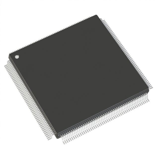
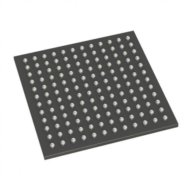
A3P400-2FGG256
| Part Description |
ProASIC3 Field Programmable Gate Array (FPGA) IC 178 55296 256-LBGA |
|---|---|
| Quantity | 1,383 Available (as of June 10, 2026) |

| Product Category | Field Programmable Gate Array (FPGA) |
|---|---|
| Manufacturer | Microchip Technology |
| Manufacturing Status | Active |
| Manufacturer Standard Lead Time | 8 Weeks |
| Datasheet |
Specifications & Environmental
| Device Package | 256-FPBGA (17x17) | Grade | Commercial | Operating Temperature | 0°C – 85°C | ||
|---|---|---|---|---|---|---|---|
| Package / Case | 256-LBGA | Number of I/O | 178 | Voltage | 1.425 V - 1.575 V | ||
| Mounting Method | Surface Mount | RoHS Compliance | ROHS3 Compliant | REACH Compliance | REACH Unaffected | ||
| Moisture Sensitivity Level | 3 (168 Hours) | Number of LABs/CLBs | 9216 | Number of Logic Elements/Cells | 9216 | ||
| Number of Gates | 400000 | ECCN | 3A991D | HTS Code | 8542.39.0001 | ||
| Qualification | N/A | Total RAM Bits | 55296 |
Overview of A3P400-2FGG256 – ProASIC3 FPGA, 256-LBGA, 178 I/O
The A3P400-2FGG256 is a ProASIC3 field programmable gate array (FPGA) from Microchip Technology. It provides 9,216 logic elements (cells), approximately 55 Kbits of on-chip RAM, and 178 general-purpose I/O pins in a 256-ball BGA package.
Designed for surface-mount placement and commercial-temperature operation, this device is suited to designs that require programmable logic capacity with a defined operating voltage range and package footprint.
Key Features
- Logic Capacity 9,216 logic elements (cells) and approximately 400,000 equivalent gates to implement custom digital functions and moderate-complexity state machines.
- On‑Chip Memory Total embedded memory of 55,296 bits (approximately 55 Kbits) to support buffering, small lookup tables, and local data storage.
- I/O Resources 178 available I/O pins for interfacing with peripherals, sensors, and external logic devices.
- Power Specified supply voltage range of 1.425 V to 1.575 V to match systems designed around this core voltage.
- Package & Mounting 256-ball LBGA package (supplier device package: 256-FPBGA, 17×17) with surface-mount mounting suitable for modern PCB assembly processes.
- Operating Range Commercial temperature grade with an operating range of 0 °C to 85 °C.
- Compliance RoHS compliant, meeting common lead-free environmental requirements.
Typical Applications
- Embedded Control Implement custom control logic, state machines, and protocol bridging where 9,216 logic elements and 178 I/O provide required resources.
- Interface and Glue Logic Consolidate discrete logic functions and manage multiple peripheral interfaces using available I/O and on-chip memory.
- Data Acquisition Buffer and preprocess sensor or peripheral data with on-chip RAM and programmable logic before handing off to a host processor.
Unique Advantages
- Defined Logic Density: 9,216 logic elements and 400,000 gates give clear implementation capacity for designers planning resource budgets.
- On‑Chip Memory for Local Storage: Approximately 55 Kbits of embedded RAM reduces dependence on external memory for small buffers and LUTs.
- Generous I/O Count: 178 I/O pins enable flexible interfacing to multiple subsystems without additional I/O expanders.
- Standard BGA Package: 256-ball LBGA (256-FPBGA 17×17) provides a compact, production-friendly footprint for modern PCBs.
- Predictable Power Envelope: A specified supply range of 1.425 V to 1.575 V supports consistent power design and verification.
- RoHS Compliant: Conforms to lead‑free environmental requirements for streamlined qualification in many markets.
Why Choose A3P400-2FGG256?
The A3P400-2FGG256 offers a clearly defined combination of logic capacity, on‑chip memory, and I/O count in a compact 256-ball BGA package from Microchip Technology. Its documented operating voltage and commercial temperature range make it suitable for a wide range of embedded and interface-focused designs that require programmable logic within these parameters.
This part is appropriate for teams and designs that need transparent resource sizing (logic elements, gates, RAM, and I/O) and prefer an FPGA solution packaged for surface-mount assembly with RoHS compliance. It provides a straightforward platform for implementing custom digital functions while aligning with established PCB and power design constraints.
Request a quote or submit an inquiry for pricing and availability to evaluate the A3P400-2FGG256 for your next design.


Date Founded: 1989
Headquarters: Chandler, Arizona, USA
Employees: 22,000+
Revenue: $8.349 Billion
Certifications and Memberships: ISO9001:2015, IATF16949:2016, AS 9100D


