
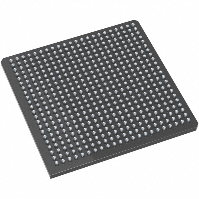
A3PE3000-FGG484
| Part Description |
ProASIC3E Field Programmable Gate Array (FPGA) IC 341 516096 484-BGA |
|---|---|
| Quantity | 43 Available (as of June 14, 2026) |
| Product Category | Field Programmable Gate Array (FPGA) |
|---|---|
| Manufacturer | Microchip Technology |
| Manufacturing Status | Active |
| Manufacturer Standard Lead Time | 8 Weeks |
| Datasheet |
Specifications & Environmental
| Device Package | 484-FPBGA (23x23) | Grade | Commercial | Operating Temperature | 0°C – 85°C | ||
|---|---|---|---|---|---|---|---|
| Package / Case | 484-BGA | Number of I/O | 341 | Voltage | 1.425 V - 1.575 V | ||
| Mounting Method | Surface Mount | RoHS Compliance | ROHS3 Compliant | REACH Compliance | REACH Unaffected | ||
| Moisture Sensitivity Level | 3 (168 Hours) | Number of LABs/CLBs | 75264 | Number of Logic Elements/Cells | 75264 | ||
| Number of Gates | 3000000 | ECCN | 3A991D | HTS Code | 8542.39.0001 | ||
| Qualification | N/A | Total RAM Bits | 516096 |
Overview of A3PE3000-FGG484 – ProASIC3E FPGA, 341 I/O, 484-BGA
The A3PE3000-FGG484 is a ProASIC3E Field Programmable Gate Array (FPGA) IC from Microchip Technology designed for applications that require substantial logic capacity and I/O density in a compact BGA package. It combines 75,264 logic elements with approximately 0.516 Mbits of embedded memory and 3,000,000 gates, offering a balanced platform for custom digital logic, high-density interfacing and on-chip data buffering.
Supplied in a 484-FPBGA (23×23) surface-mount package, this commercially graded, RoHS-compliant device operates across a 1.425 V to 1.575 V core supply range and an operating temperature range of 0°C to 85°C.
Key Features
- Logic Capacity 75,264 logic elements (cells) and approximately 3,000,000 gates provide substantial programmable logic resources for complex designs.
- Embedded Memory Approximately 0.516 Mbits of on-chip RAM to support data buffering, FIFOs and small working storage without external memory.
- I/O Density 341 user I/O pins to support wide parallel interfaces, multiple peripherals or mixed-signal front-end routing.
- Package and Mounting 484-FPBGA (23×23) package case in a surface-mount form factor for compact board-level integration and reliable solder mounting.
- Power Core voltage supply range of 1.425 V to 1.575 V to match designs targeting that Vcore envelope.
- Operating Range and Grade Commercial-grade device rated for 0°C to 85°C operation; RoHS-compliant for lead-free assembly.
Typical Applications
- Custom Logic and Control Systems requiring extensive programmable logic resources—up to 75,264 logic elements—can implement complex state machines and control functions on-chip.
- I/O-Intensive Designs Applications that need large numbers of external interfaces benefit from the device’s 341 available I/O pins for parallel buses and multiple peripherals.
- On-Chip Buffering and Small Data Stores Designs that use embedded memory for buffering, FIFOs or temporary storage can leverage approximately 0.516 Mbits of on-chip RAM.
- Compact Board-Level Integration The 484-FPBGA (23×23) surface-mount package fits applications where board space and package density are important considerations.
Unique Advantages
- High Logic Density: The combination of 75,264 logic elements and 3,000,000 gates enables consolidation of multiple functions into a single FPGA, reducing external component count.
- Significant I/O Capacity: With 341 I/O pins, the device supports broad connectivity options without additional I/O expanders, simplifying system design.
- Integrated Memory: Approximately 0.516 Mbits of embedded RAM reduces dependence on external memory for small to moderate buffering needs.
- Compact BGA Packaging: The 484-FPBGA (23×23) package offers a high-pin-count solution in a compact footprint suitable for dense board layouts.
- Commercial Operating Range: Rated for 0°C to 85°C operation and RoHS-compliant to support standard commercial product requirements.
Why Choose A3PE3000-FGG484?
The A3PE3000-FGG484 positions itself as a balanced FPGA option where significant logic resources, a large number of I/Os, and on-chip memory are required within a compact BGA footprint. Its combination of 75,264 logic elements, ~0.516 Mbits of RAM and 341 I/O pins makes it suitable for designers seeking to integrate multiple digital functions and interfaces into a single device while maintaining a commercial-grade operating profile.
This device delivers measurable board-level benefits—reduced external components, consolidated I/O routing and on-chip buffering—while meeting RoHS requirements and typical commercial temperature ranges, supporting medium- to high-density embedded designs.
Request a quote or submit a parts inquiry to receive pricing and availability for the A3PE3000-FGG484.


Date Founded: 1989
Headquarters: Chandler, Arizona, USA
Employees: 22,000+
Revenue: $8.349 Billion
Certifications and Memberships: ISO9001:2015, IATF16949:2016, AS 9100D


