
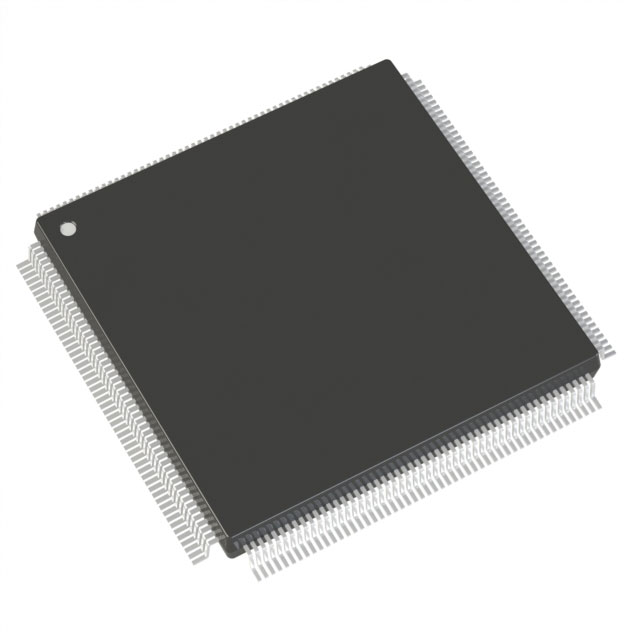
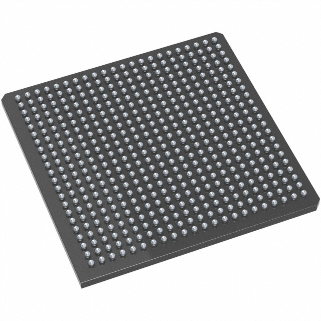
A3PE3000-FGG896
| Part Description |
ProASIC3E Field Programmable Gate Array (FPGA) IC 620 516096 896-BGA |
|---|---|
| Quantity | 789 Available (as of June 15, 2026) |

| Product Category | Field Programmable Gate Array (FPGA) |
|---|---|
| Manufacturer | Microchip Technology |
| Manufacturing Status | Active |
| Manufacturer Standard Lead Time | 8 Weeks |
| Datasheet |
Specifications & Environmental
| Device Package | 896-FBGA (31x31) | Grade | Commercial | Operating Temperature | 0°C – 85°C | ||
|---|---|---|---|---|---|---|---|
| Package / Case | 896-BGA | Number of I/O | 620 | Voltage | 1.425 V - 1.575 V | ||
| Mounting Method | Surface Mount | RoHS Compliance | ROHS3 Compliant | REACH Compliance | REACH Unaffected | ||
| Moisture Sensitivity Level | 3 (168 Hours) | Number of LABs/CLBs | 75264 | Number of Logic Elements/Cells | 75264 | ||
| Number of Gates | 3000000 | ECCN | 3A001A7A | HTS Code | 8542.39.0001 | ||
| Qualification | N/A | Total RAM Bits | 516096 |
Overview of A3PE3000-FGG896 – ProASIC3E Field Programmable Gate Array (FPGA) IC, 896-FBGA (31×31)
The A3PE3000-FGG896 is a ProASIC3E Field Programmable Gate Array (FPGA) IC supplied in an 896-FBGA (31×31) package with surface-mount mounting. It provides 75,264 logic elements, approximately 0.516 Mbits of embedded memory, and 620 I/Os for designs that require substantial logic capacity and high I/O density.
Operating from a core supply range of 1.425 V to 1.575 V and rated for commercial temperature operation from 0 °C to 85 °C, the device offers a compact, RoHS-compliant programmable logic option for a wide range of commercial electronic applications.
Key Features
- Logic Capacity Provides 75,264 logic elements (cells) supporting complex programmable logic implementations and moderate gate counts.
- Embedded Memory Approximately 0.516 Mbits of on-chip RAM to support buffering, FIFOs, and small data-storage functions within logic designs.
- I/O Density 620 I/O pins enable multi-channel interfacing and extensive peripheral connectivity in a single FPGA package.
- Gate Count Rated for 3,000,000 gates, supplying a clear indicator of overall logic resource scale for partitioning and integration planning.
- Package & Mounting 896-FBGA (31×31) package, surface-mount mounting type, suitable where a high pin-count BGA form factor is required.
- Power Core supply range of 1.425 V to 1.575 V to match system power domains and design constraints.
- Operating Conditions Commercial grade device rated for 0 °C to 85 °C operating temperature.
- Environmental Compliance RoHS compliant, supporting regulatory environmental requirements for lead-free manufacturing.
Typical Applications
- High‑I/O Interface Control Leverage the 620 I/Os to manage multiple parallel interfaces, protocol bridges, or dense connector-based systems.
- Embedded Logic and Glue Use the 75,264 logic elements to implement custom control logic, timing-critical glue logic, or data-path processing within system designs.
- On‑Chip Buffering Employ approximately 0.516 Mbits of embedded RAM for buffering, small FIFOs, or temporary data storage in stream-handling applications.
Unique Advantages
- High Logic Density: 75,264 logic elements provide substantial programmable resources for mid‑to‑large designs without external CPLDs or multiple devices.
- Large I/O Count: 620 I/Os reduce the need for external I/O expanders and simplify multi‑lane or multi‑peripheral designs.
- Integrated Memory: Approximately 0.516 Mbits of embedded RAM enables local buffering and state storage, improving throughput and simplifying external memory usage.
- Compact High‑Pin Package: 896-FBGA (31×31) delivers high connection density in a single surface-mount package to conserve board area.
- Defined Power Window: Core voltage range of 1.425 V to 1.575 V supports consistent power budgeting and regulator selection.
- RoHS Compliance: Meets lead‑free manufacturing requirements for environmentally compliant production.
Why Choose A3PE3000-FGG896?
The A3PE3000-FGG896 balances substantial logic resources, embedded memory, and a very high I/O count in a single 896‑FBGA surface‑mount package. Its commercial temperature grade and defined core voltage range make it suitable for a range of commercial electronic designs where integration density and I/O capability are priorities.
This device is well suited to engineers and purchasers looking for a programmable logic solution that consolidates multiple functions—control logic, interfacing, and buffering—into one component, reducing BOM complexity and board-level routing compared with multi-device solutions.
If you would like pricing or availability, request a quote or submit your requirements and a sales specialist will provide a formal quote and lead‑time information.


Date Founded: 1989
Headquarters: Chandler, Arizona, USA
Employees: 22,000+
Revenue: $8.349 Billion
Certifications and Memberships: ISO9001:2015, IATF16949:2016, AS 9100D


