
AFS250-FG256I
| Part Description |
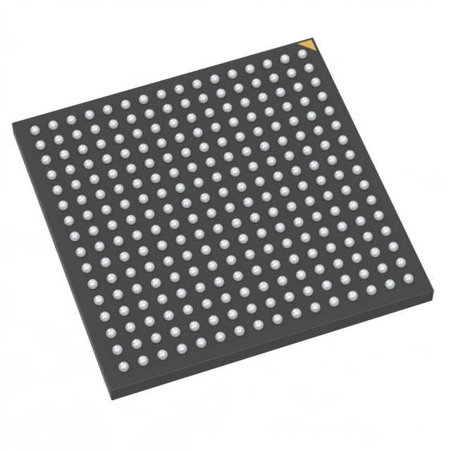
Fusion® Field Programmable Gate Array (FPGA) IC 114 36864 256-LBGA |
|---|---|
| Quantity | 1,466 Available (as of June 15, 2026) |

| Product Category | Field Programmable Gate Array (FPGA) |
|---|---|
| Manufacturer | Microchip Technology |
| Manufacturing Status | Active |
| Manufacturer Standard Lead Time | 14 Weeks |
| Datasheet |
Specifications & Environmental
| Device Package | 256-FPBGA (17x17) | Grade | Industrial | Operating Temperature | -40°C – 100°C | ||
|---|---|---|---|---|---|---|---|
| Package / Case | 256-LBGA | Number of I/O | 114 | Voltage | 1.425 V - 1.575 V | ||
| Mounting Method | Surface Mount | RoHS Compliance | RoHS non-compliant | REACH Compliance | REACH Unaffected | ||
| Moisture Sensitivity Level | 3 (168 Hours) | Number of LABs/CLBs | 6144 | Number of Logic Elements/Cells | 6144 | ||
| Number of Gates | 250000 | ECCN | 3A991D | HTS Code | 8542.39.0001 | ||
| Qualification | N/A | Total RAM Bits | 36864 |
Overview of AFS250-FG256I – Fusion® Field Programmable Gate Array (FPGA) IC 114 36864 256-LBGA
The AFS250-FG256I is a Fusion® Field Programmable Gate Array (FPGA) offered by Microchip Technology. It provides a balanced integration of programmable logic, on-chip memory and I/O resources in a compact 256-ball LBGA package targeted at industrial applications.
With 6,144 logic elements, approximately 36.9 kbits of embedded memory and 114 user I/O pins, the device is suited for designs that require moderate programmable logic capacity, deterministic voltage supply requirements and extended operating temperature range.
Key Features
- Core Logic 6,144 logic elements and approximately 250,000 gates provide the programmable logic resources for custom digital functions and state machines.
- Embedded Memory Approximately 36.9 kbits of on-chip RAM (36,864 bits) for buffering, small data structures or LUT-based storage within user designs.
- I/O Count 114 user I/O pins to interface with sensors, peripherals and external devices in multi-signal systems.
- Package and Mounting 256-LBGA package (supplier package: 256-FPBGA, 17×17) designed for surface-mount assembly in space-constrained boards.
- Power Specified supply voltage range of 1.425 V to 1.575 V for the core supply to support predictable system power budgeting and design.
- Temperature and Grade Industrial-grade device specified for operation from −40 °C to 100 °C, allowing deployment in a wide range of industrial environments.
- Regulatory Compliance RoHS-compliant to align with common environmental requirements for electronic assemblies.
Typical Applications
- Industrial Control and Automation — Leverage the industrial temperature rating and 114 I/O to implement sensor aggregation, motor control interfaces and custom control logic.
- Embedded Glue Logic — Use the available logic elements and on-chip RAM to combine functions, protocol conversion and timing logic in compact systems.
- Sensor and I/O Aggregation — The mix of I/O and logic resources supports aggregation, preprocessing and interfacing of multiple sensor signals before passing data to a host processor.
- Industrial Communication Interfaces — Implement deterministic, application-specific communication or bridging functions using the programmable logic and I/O resources.
Unique Advantages
- Moderate Logic Capacity: 6,144 logic elements enable substantial custom digital functions while keeping device complexity manageable for mid-size designs.
- Integrated On-Chip Memory: Approximately 36.9 kbits of embedded RAM reduces the need for external buffering in many control and interface tasks.
- Generous I/O Count: 114 user I/O pins provide flexibility for connecting multiple peripherals, sensors and user interfaces without additional components.
- Compact Surface-Mount Package: 256-LBGA (256-FPBGA, 17×17) minimizes PCB area while supporting robust assembly processes.
- Industrial Temperature Support: Rated from −40 °C to 100 °C to meet thermal requirements of factory, process and field-deployed equipment.
- RoHS Compliance: Environmentally compliant construction simplifies regulatory alignment for product builds.
Why Choose AFS250-FG256I?
The AFS250-FG256I positions itself as a reliable, industrial-grade FPGA option for mid-sized embedded designs where a balance of programmable logic, on-chip memory and I/O density is required. Its specified core voltage range and compact 256-LBGA package make it suitable for space-constrained boards that need predictable power and thermal behavior.
This part is well suited to engineers developing industrial control systems, I/O aggregation modules, protocol bridges and embedded glue logic that benefit from on-chip memory and a significant number of user I/Os. Choosing this device offers a straightforward path to integrate configurable digital functionality while keeping BOM and board area under control.
Request a quote or submit a request for pricing and availability for the AFS250-FG256I to begin procurement or to discuss volume needs.


Date Founded: 1989
Headquarters: Chandler, Arizona, USA
Employees: 22,000+
Revenue: $8.349 Billion
Certifications and Memberships: ISO9001:2015, IATF16949:2016, AS 9100D


