
AFS250-FGG256
| Part Description |
Fusion® Field Programmable Gate Array (FPGA) IC 114 36864 256-LBGA |
|---|---|
| Quantity | 1,006 Available (as of June 18, 2026) |

| Product Category | Field Programmable Gate Array (FPGA) |
|---|---|
| Manufacturer | Microchip Technology |
| Manufacturing Status | Active |
| Manufacturer Standard Lead Time | 14 Weeks |
| Datasheet |
Specifications & Environmental
| Device Package | 256-FPBGA (17x17) | Grade | Commercial | Operating Temperature | 0°C – 85°C | ||
|---|---|---|---|---|---|---|---|
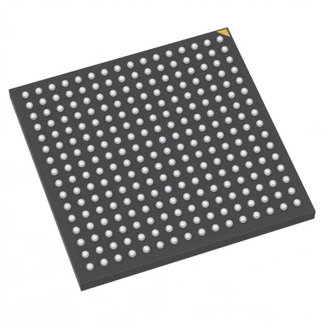
| Package / Case | 256-LBGA | Number of I/O | 114 | Voltage | 1.425 V - 1.575 V | ||
| Mounting Method | Surface Mount | RoHS Compliance | ROHS3 Compliant | REACH Compliance | REACH Unaffected | ||
| Moisture Sensitivity Level | 3 (168 Hours) | Number of LABs/CLBs | 6144 | Number of Logic Elements/Cells | 6144 | ||
| Number of Gates | 250000 | ECCN | 3A991D | HTS Code | 8542.39.0001 | ||
| Qualification | N/A | Total RAM Bits | 36864 |
Overview of AFS250-FGG256 – Fusion® Field Programmable Gate Array (FPGA), 250,000 gates, 256-LBGA
The AFS250-FGG256 is a Fusion® Field Programmable Gate Array (FPGA) IC providing programmable logic, embedded memory, and a broad set of I/O in a compact BGA package. It delivers 6,144 logic elements and approximately 36,864 bits (≈0.037 Mbits) of on-chip RAM, suited to commercial electronic designs that require moderate logic density and configurable interfaces.
Key attributes include 114 I/O pins, a supply voltage range of 1.425 V to 1.575 V, and a commercial operating temperature range of 0 °C to 85 °C, supplied in a 256-ball FPBGA (17×17) surface-mount package.
Key Features
- Core Logic 6,144 logic elements providing a practical programmable fabric for custom logic, control functions, and glue logic.
- Logic Capacity Reported 250,000 gates, enabling implementation of moderate-complexity designs within a single device.
- Embedded Memory Approximately 36,864 bits of on-chip RAM for temporary storage, buffering, and small lookup tables.
- I/O 114 user I/O pins to interface with peripherals, sensors, and external logic in board-level designs.
- Power Operates from a core supply of 1.425 V to 1.575 V to match low-voltage system rails.
- Package & Mounting 256-ball FPBGA (256-LBGA) surface-mount package, supplier package specified as 256-FPBGA (17×17).
- Temperature & Grade Commercial grade operation from 0 °C to 85 °C for standard commercial electronics applications.
- Environmental Compliance RoHS compliant for lead-free, environmentally conscious assembly and production processes.
Typical Applications
- Commercial Embedded Systems — Implement custom control logic, protocol handling, or interface bridging inside commercial electronic products.
- Prototyping and Development — Rapidly iterate hardware functionality and validate logic before committing to fixed-function ASICs or SoCs.
- User Interfaces and Control — Drive and manage peripheral I/O, button/key scanning, and simple display/control logic using the available I/O and on-chip resources.
Unique Advantages
- Balanced Logic Density: 6,144 logic elements and 250,000 gates provide a middle-ground capacity for many commercial designs without excessive cost or board area.
- Integrated Memory: On-chip RAM (36,864 bits) reduces the need for small external memory components for buffering and LUTs.
- Generous I/O Count: 114 I/O pins allow direct interfacing to a variety of peripherals and external logic devices.
- Compact BGA Packaging: 256-ball FPBGA (17×17) surface-mount package minimizes PCB footprint while enabling reliable soldered connections.
- Low-Voltage Core: Core supply specified between 1.425 V and 1.575 V to align with low-voltage system architectures.
- RoHS Compliant: Meets lead-free environmental requirements for modern electronics manufacturing.
Why Choose AFS250-FGG256?
The AFS250-FGG256 positions itself as a compact, commercial-grade FPGA option for designers who need moderate programmable logic, embedded RAM, and substantial I/O in a small BGA package. Its combination of 6,144 logic elements, approximately 36.9 kbits of embedded memory, and 114 I/O pins makes it well suited for a range of commercial applications where board space, reconfigurability, and environmental compliance matter.
Choose this device when your design requires scalable programmable logic with a predictable operating voltage and commercial temperature range, supported by a surface-mount 256-ball FPBGA package for dense PCB integration.
Request a quote or submit an inquiry to receive pricing, availability, and lead-time information for AFS250-FGG256.


Date Founded: 1989
Headquarters: Chandler, Arizona, USA
Employees: 22,000+
Revenue: $8.349 Billion
Certifications and Memberships: ISO9001:2015, IATF16949:2016, AS 9100D


