
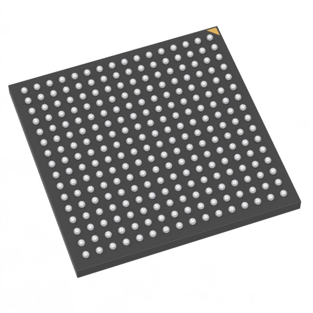
AFS250-FG256
| Part Description |
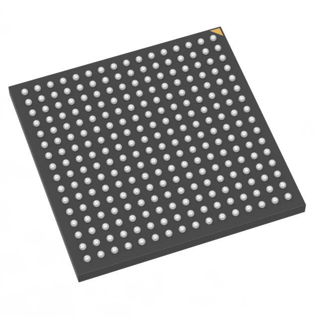
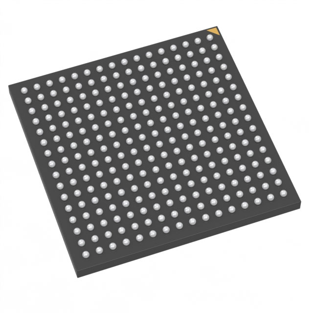
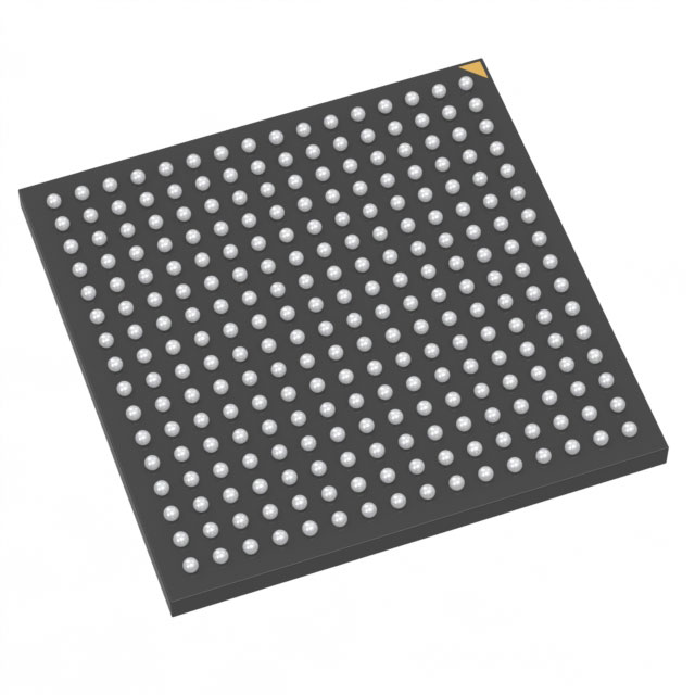
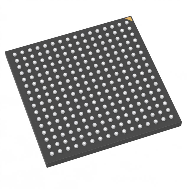
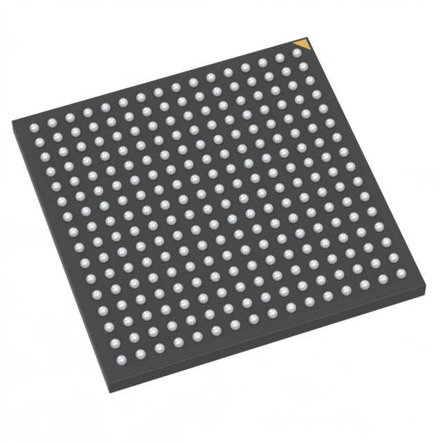
Fusion® Field Programmable Gate Array (FPGA) IC 114 36864 256-LBGA |
|---|---|
| Quantity | 387 Available (as of October 8, 2026) |
| Product Category | Field Programmable Gate Array (FPGA) |
|---|---|
| Manufacturer | Microchip Technology |
| Manufacturing Status | Active |
| Manufacturer Standard Lead Time | 14 Weeks |
| Datasheet |
Specifications & Environmental
| Device Package | 256-FPBGA (17x17) | Grade | Commercial | Operating Temperature | 0°C – 85°C | ||
|---|---|---|---|---|---|---|---|
| Package / Case | 256-LBGA | Number of I/O | 114 | Voltage | 1.425 V - 1.575 V | ||
| Mounting Method | Surface Mount | RoHS Compliance | RoHS non-compliant | REACH Compliance | REACH Unaffected | ||
| Moisture Sensitivity Level | 3 (168 Hours) | Number of LABs/CLBs | 6144 | Number of Logic Elements/Cells | 6144 | ||
| Number of Gates | 250000 | ECCN | 3A991D | HTS Code | 8542.39.0001 | ||
| Qualification | N/A | Total RAM Bits | 36864 |
Overview of AFS250-FG256 – Fusion® Field Programmable Gate Array (FPGA) IC 114 36864 256-LBGA
The AFS250-FG256 is a Fusion® field programmable gate array (FPGA) from Microchip Technology designed for commercial embedded applications. It provides a balance of logic capacity, on-chip memory and flexible I/O in a compact 256-LBGA package.
Built with 6,144 logic elements and approximately 36,864 bits of embedded memory, this FPGA targets commercial designs that require configurable logic, moderate on-chip RAM and a sizable I/O count while operating within a 1.425 V to 1.575 V core supply range and a 0 °C to 85 °C temperature window.
Key Features
- Logic Capacity 6,144 logic elements supporting approximately 250,000 gates for implementing custom digital logic and control functions.
- Embedded Memory 36,864 bits of on-chip RAM (approximately 0.037 Mbits) for local buffering, small data tables and state storage.
- I/O Resources 114 general-purpose I/O pins to support diverse interfaces and signal connections in compact systems.
- Power Core voltage supply range of 1.425 V to 1.575 V, enabling integration with low-voltage system rails.
- Package & Mounting 256-LBGA (supplier package: 256-FPBGA, 17×17) in a surface-mount form factor for space-constrained boards.
- Operating Range Commercial-grade operating temperature from 0 °C to 85 °C suitable for commercial and consumer applications.
- Compliance RoHS compliant.
Typical Applications
- Commercial Embedded Systems Use the FPGA for control logic, protocol handling and custom interfaces in commercial electronics where moderate logic and memory are sufficient.
- Interface Bridging Implement custom I/O bridges and signal adaptors leveraging 114 I/O pins to connect disparate peripherals and buses.
- Prototyping and Development Ideal for developers building and validating configurable logic functions and proof-of-concept designs in a commercial environment.
- Test and Measurement Equipment Employ the device for deterministic logic, data capture and preprocessing tasks that benefit from on-chip RAM and programmable logic.
Unique Advantages
- Balanced Logic Density: 6,144 logic elements and ~250,000 gates provide sufficient capacity for a wide range of mid-range logic designs without excess overhead.
- On-chip Memory for Local Data: 36,864 bits of embedded RAM enable localized buffering and small lookup tables, reducing external memory needs.
- High I/O Count: 114 I/O pins simplify system-level integration and allow direct connections to multiple peripherals and sensors.
- Compact, Surface-Mount Package: 256-LBGA (17×17 FPBGA) minimizes board area while keeping routing manageable for dense designs.
- Low-Voltage Core: Narrow core supply range (1.425 V–1.575 V) supports designs using low-voltage power rails for reduced power dissipation.
- Commercial Temperature Suitability: Rated for 0 °C to 85 °C, matching the environmental expectations of commercial and consumer product designs.
Why Choose AFS250-FG256?
The AFS250-FG256 positions itself as a compact, commercially graded FPGA option that combines moderate logic capacity, embedded memory and a generous I/O count in a space-efficient 256-LBGA package. Its specifications make it suitable for designers needing programmable logic and local RAM in commercial embedded systems, interface bridging, prototyping and test equipment.
Backed by Microchip Technology, the device offers a clear balance of integration and predictable operating parameters—making it a practical choice for teams focused on scalable, maintainable designs that require FPGA configurability without industrial or automotive-level qualification.
Request a quote or submit a pricing inquiry to obtain availability, lead time and volume pricing for the AFS250-FG256.





















Date Founded: 1989
Headquarters: Chandler, Arizona, USA
Employees: 22,000+
Revenue: $8.349 Billion
Certifications and Memberships: ISO9001:2015, IATF16949:2016, AS 9100D




