
AGL600V2-CSG281I
| Part Description |
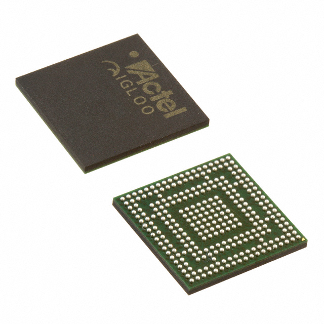
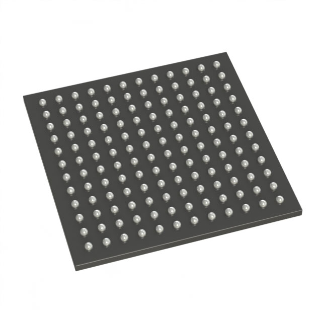
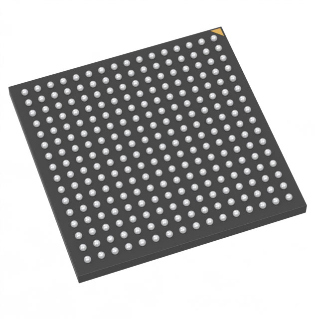
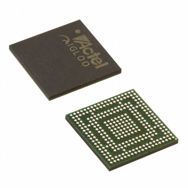
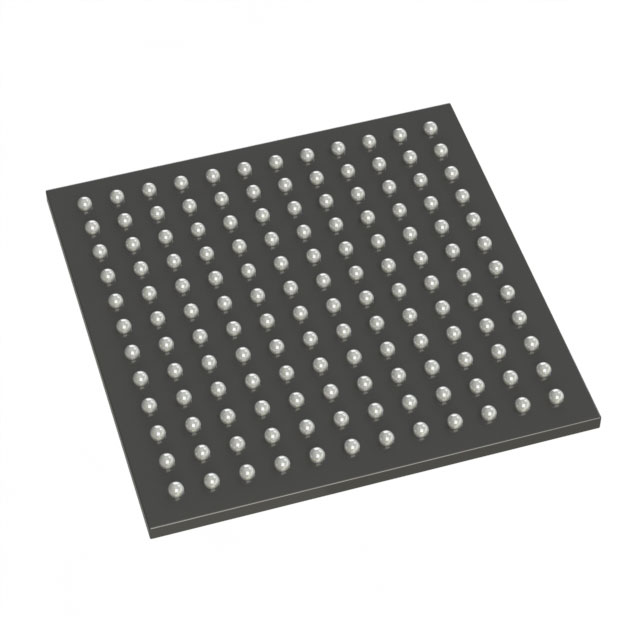
IGLOO Field Programmable Gate Array (FPGA) IC 215 110592 13824 281-TFBGA, CSBGA |
|---|---|
| Quantity | 874 Available (as of October 7, 2026) |
| Product Category | Field Programmable Gate Array (FPGA) |
|---|---|
| Manufacturer | Microchip Technology |
| Manufacturing Status | Active |
| Manufacturer Standard Lead Time | 8 Weeks |
| Datasheet |
Specifications & Environmental
| Device Package | 281-CSP (10x10) | Grade | Industrial | Operating Temperature | -40°C – 85°C | ||
|---|---|---|---|---|---|---|---|
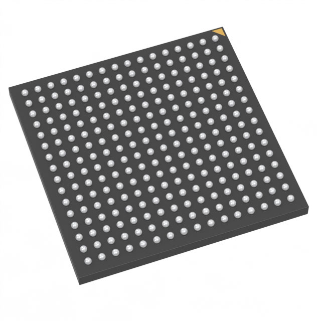
| Package / Case | 281-TFBGA, CSBGA | Number of I/O | 215 | Voltage | 1.14 V - 1.575 V | ||
| Mounting Method | Surface Mount | RoHS Compliance | ROHS3 Compliant | REACH Compliance | REACH Unaffected | ||
| Moisture Sensitivity Level | 3 (168 Hours) | Number of LABs/CLBs | 13824 | Number of Logic Elements/Cells | 13824 | ||
| Number of Gates | 600000 | ECCN | 3A991D | HTS Code | 8542.39.0001 | ||
| Qualification | N/A | Total RAM Bits | 110592 |
Overview of AGL600V2-CSG281I – IGLOO Field Programmable Gate Array, 215 I/Os, 281-TFBGA
The AGL600V2-CSG281I is an IGLOO flash-based Field Programmable Gate Array (FPGA) in a 281-TFBGA (CSBGA) package designed for industrial applications. Built on the IGLOO low-power flash FPGA architecture, it delivers reprogrammable nonvolatile logic with low standby and active power modes for compact, power-efficient embedded and industrial designs.
Key on-chip resources include 13,824 logic elements, approximately 0.11 Mbits of embedded RAM, and 215 user I/Os, providing a balance of density, I/O capacity, and low-power operation for control, I/O bridging, and system-power-management applications.
Key Features
- Programmable Logic — 13,824 logic elements (cells) supporting designs up to 600,000 system gates, enabling medium-density FPGA implementations.
- Embedded Memory — Total on-chip RAM of 110,592 bits (approximately 0.11 Mbits) for user data and buffering.
- I/O Capacity & Flexibility — 215 user I/Os with bank-selectable voltages and mixed-voltage operation, suitable for interfacing diverse peripherals and signal standards.
- Low-Power Operation — Flash*Freeze ultra-low-power mode (as low as 5 μW) and Low Power Active capability (from 12 μW) to minimize system standby and enable energy-aware designs.
- Nonvolatile Flash Technology — Flash-based FPGA fabric that retains programmed design when powered off and supports reprogramming for field updates.
- Clocking and Timing — Integrated clock conditioning blocks with one block including a PLL; series-level system performance up to 250 MHz (1.5 V systems) and 160 MHz (1.2 V systems).
- Security & In-System Programming — Supports in-system programming with on-chip 128-bit AES decryption and FlashLock for protecting FPGA content (series feature).
- Industrial Grade and Packaging — Industrial operating temperature range of −40 °C to 85 °C, supplied in a 281-TFBGA / 281-CSP (10×10) surface-mount package; RoHS compliant.
- Supply Voltage — Core and related supply support in the range of 1.14 V to 1.575 V for low-voltage system integration.
Typical Applications
- Industrial Control — Implement motor control logic, deterministic state machines, and sensor aggregation in industrial systems that require industrial temperature range and robust I/O.
- Low-Power Embedded Systems — Use Flash*Freeze and Low Power Active modes to implement always-on control, wake-from-sensor tasks, and energy-sensitive monitoring functions.
- I/O Bridging and Protocol Conversion — Leverage 215 user I/Os and mixed-voltage bank support to build interface bridges and protocol translators between legacy and modern subsystems.
- Secure In-System Programmable Logic — Deploy reprogrammable logic with on-chip AES-based ISP and FlashLock features for field updates with content protection.
Unique Advantages
- Single-Chip, Nonvolatile Solution: Flash-based fabric retains the programmed design without external configuration memory, simplifying BOM and system startup.
- Ultra-Low Standby Power: Flash*Freeze mode (as low as 5 μW) and Low Power Active operation enable designs that require minimal standby energy while retaining state.
- Balanced Resource Set: 13,824 logic elements, ~0.11 Mbits of RAM and 215 I/Os provide a versatile mix of logic, memory, and connectivity for medium-density applications.
- Industrial Readiness: Rated for −40 °C to 85 °C operating temperature and supplied in a compact 281-TFBGA package suitable for industrial PCBs and surface-mount assembly.
- Flexible Clocking: Multiple clock conditioning blocks and an integrated PLL support configurable clock management for performance and timing control.
- Protected Field Updates: Series-level support for 128-bit AES ISP and FlashLock enables secure firmware updates and IP protection in deployed systems.
Why Choose AGL600V2-CSG281I?
The AGL600V2-CSG281I provides a practical combination of low-power operation, nonvolatile reprogrammability, and a balanced set of logic, memory, and I/O resources for industrial and embedded designs. Its flash-based IGLOO architecture supports instant-on behavior and secure in-system programming while reducing the need for external configuration storage.
Choose this device when you need a compact, surface-mount FPGA with industrial temperature capability, efficient standby modes, and the flexibility to support mixed-voltage interfaces and secure field updates—helping simplify system design and long-term maintainability.
Request a quote or submit an inquiry to our sales team to discuss pricing, availability, or sample requests for the AGL600V2-CSG281I.






















Date Founded: 1989
Headquarters: Chandler, Arizona, USA
Employees: 22,000+
Revenue: $8.349 Billion
Certifications and Memberships: ISO9001:2015, IATF16949:2016, AS 9100D




