
AX2000-1CGS624M
| Part Description |
Axcelerator Field Programmable Gate Array (FPGA) IC 418 294912 624-BCCGA |
|---|---|
| Quantity | 567 Available (as of June 15, 2026) |

| Product Category | Field Programmable Gate Array (FPGA) |
|---|---|
| Manufacturer | Microchip Technology |
| Manufacturing Status | Active |
| Manufacturer Standard Lead Time | 48 Weeks |
| Datasheet |
Specifications & Environmental
| Device Package | 624-CCGA (32.5x32.5) | Grade | Military | Operating Temperature | -55°C – 125°C | ||
|---|---|---|---|---|---|---|---|
| Package / Case | 624-BCCGA | Number of I/O | 418 | Voltage | 1.425 V - 1.575 V | ||
| Mounting Method | Through Hole | RoHS Compliance | RoHS non-compliant | REACH Compliance | REACH Unaffected | ||
| Moisture Sensitivity Level | 3 (168 Hours) | Number of LABs/CLBs | 32256 | Number of Logic Elements/Cells | 32256 | ||
| Number of Gates | 2000000 | ECCN | 3A001A2C | HTS Code | 8542.39.0001 | ||
| Qualification | N/A | Total RAM Bits | 294912 |
Overview of AX2000-1CGS624M – Axcelerator Field Programmable Gate Array (FPGA) IC 418 294912 624-BCCGA
The AX2000-1CGS624M is an Axcelerator antifuse FPGA from Microchip Technology based on the AX architecture. It delivers a single-chip, nonvolatile FPGA solution with high logic capacity and embedded memory, designed for high-performance and security-conscious applications.
With 2,000,000 equivalent system gates, segmentable clocks, embedded PLLs, and on-chip SRAM/FIFO control, this device targets designs that require significant logic resources, large I/O counts and deterministic timing across a wide operating temperature range consistent with military-grade requirements.
Key Features
- Core Capacity – 2,000,000 equivalent system gates and 32,256 logic elements provide substantial on-chip logic resources for complex FPGA implementations.
- Embedded Memory – Approximately 295 kbits of embedded SRAM/FIFO with variable-aspect 4,608-bit RAM blocks and independent width-configurable read/write ports.
- I/O and Interfaces – 418 user I/Os with support for mixed-voltage operation and bank-selectable I/O standards; LVDS-capable channels up to documented rates in the datasheet and programmable drive/slew options.
- Performance – System-level performance characteristics called out in the family documentation include 350+ MHz system performance and 500+ MHz internal performance, plus high-performance embedded FIFOs.
- Clocking and PLLs – Segmentable clock resources with embedded PLLs providing a 14–200 MHz input range and frequency synthesis capabilities up to 1 GHz.
- Voltage and Power – Core supply range specified at 1.425 V to 1.575 V for the device core.
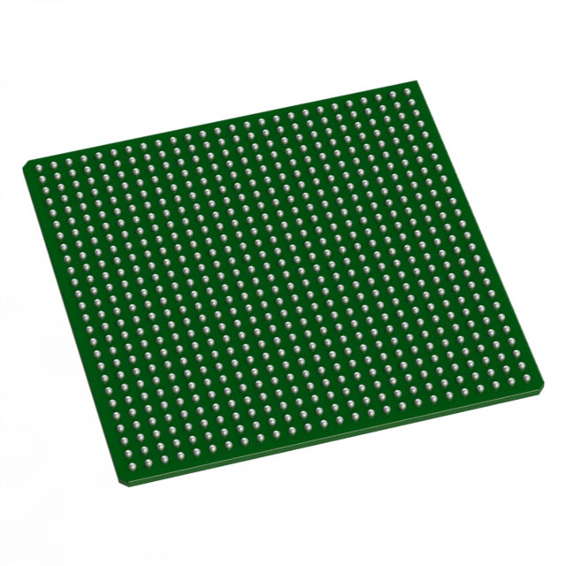
- Package and Mounting – Supplied in a 624-BCCGA package (supplier package listed as 624-CCGA, 32.5 × 32.5 mm); mounting type: through hole.
- Temperature and Grade – Military grade device with an operating temperature range of −55 °C to 125 °C.
- Security and Test – Nonvolatile single-chip antifuse solution with FuseLock™ programming protection; boundary-scan testing compliant with IEEE 1149.1 (JTAG) and in-system diagnostic/debug capability with Microchip Silicon Explorer II.
- Regulatory – RoHS compliant.
Typical Applications
- Military and Aerospace Systems – Military-grade temperature range and nonvolatile antifuse architecture make the device suitable for mission-critical electronics that require long-term configuration retention and security.
- High-Speed Data Transport – High-performance embedded FIFOs and LVDS-capable I/Os support designs requiring robust high-speed serial data handling and protocol bridging.
- Deterministic Logic and Timing – Segmentable clocks, embedded PLLs and deterministic timing controls are well suited to systems needing tight timing control and predictable latency.
- Complex System Integration – Large logic capacity and significant I/O count enable consolidation of multiple functions onto a single FPGA for reduced board-level complexity.
Unique Advantages
- Single-Chip Nonvolatile Architecture: Antifuse-based, nonvolatile configuration eliminates the need for external configuration memory and delivers inherent design security.
- High Logic and I/O Density: Two million equivalent gates with 32,256 logic elements and 418 I/Os enable integration of complex subsystems on a single device.
- Embedded Memory and FIFOs: Approximately 295 kbits of on-chip SRAM with embedded FIFO control simplifies high-throughput buffering without external memory.
- Designed for Secure Deployments: FuseLock programming technology and in-system diagnostic tools provide protection against reverse engineering and assist design validation.
- Robust Operating Range: Military-grade temperature rating (−55 °C to 125 °C) supports use in harsh environments where extended thermal tolerance is required.
- Flexible Clocking: Segmentable clocks and embedded PLLs with wide input range and high-frequency synthesis capability enable advanced timing architectures.
Why Choose AX2000-1CGS624M?
The AX2000-1CGS624M positions itself as a high-capacity, secure, and thermally robust FPGA for applications that demand nonvolatile configuration, significant on-chip logic and memory, and a large, flexible I/O estate. Its antifuse-based architecture combined with FuseLock protection and in-system debug facilities supports long-lived, secure deployments.
This device is a fit for designers consolidating complex subsystems into a single FPGA in environments that require wide temperature tolerance and secure configuration retention. The combination of embedded memory, high-performance FIFOs, programmable I/Os and PLL-based clocking provides a foundation for deterministic, high-throughput designs.
Request a quote or submit a request to receive pricing and availability for AX2000-1CGS624M.


Date Founded: 1989
Headquarters: Chandler, Arizona, USA
Employees: 22,000+
Revenue: $8.349 Billion
Certifications and Memberships: ISO9001:2015, IATF16949:2016, AS 9100D


