
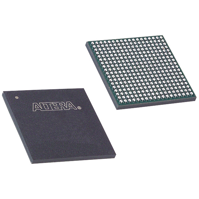
EP1C12F324C8NGA
| Part Description |
Cyclone® Field Programmable Gate Array (FPGA) IC 249 239616 12060 324-BGA |
|---|---|
| Quantity | 20 Available (as of June 15, 2026) |

| Product Category | Field Programmable Gate Array (FPGA) |
|---|---|
| Manufacturer | Intel |
| Manufacturing Status | Obsolete |
| Manufacturer Standard Lead Time | Contact Us |
| Datasheet |
Specifications & Environmental
| Device Package | 324-FBGA (19x19) | Grade | Commercial | Operating Temperature | 0°C – 85°C | ||
|---|---|---|---|---|---|---|---|
| Package / Case | 324-BGA | Number of I/O | 249 | Voltage | 1.425 V - 1.575 V | ||
| Mounting Method | Surface Mount | RoHS Compliance | Unknown | REACH Compliance | REACH Unknown | ||
| Moisture Sensitivity Level | 3 (168 Hours) | Number of LABs/CLBs | 1206 | Number of Logic Elements/Cells | 12060 | ||
| Number of Gates | N/A | ECCN | OBSOLETE | HTS Code | 0000.00.0000 | ||
| Qualification | N/A | Total RAM Bits | 239616 |
Overview of EP1C12F324C8NGA – Cyclone FPGA, 12,060 logic elements, 249 I/O, 324‑BGA
The EP1C12F324C8NGA is an Intel Cyclone® field‑programmable gate array (FPGA) in a 324‑FBGA package designed for commercial applications that require flexible, programmable logic and I/O integration. It delivers 12,060 logic elements, approximately 239,616 bits of embedded memory, and up to 249 user I/O pins to address data‑path, interface, and custom logic requirements.
Built on the Cyclone device family architecture, this device supports common memory and I/O interfaces and includes on‑chip clocking resources, providing a compact, programmable platform for system designers targeting midrange FPGA capacity in a surface‑mount BGA package.
Key Features
- Logic Capacity – 12,060 logic elements for implementing midrange programmable logic and custom datapaths.
- Embedded Memory – Approximately 239,616 bits (≈0.24 Mbits) of on‑chip RAM to support buffers, FIFOs, and small on‑chip storage.
- I/O Density – Up to 249 user I/O pins, enabling broad external connectivity and peripheral interfacing.
- Clocking – Family support for up to two PLLs for clock multiplication and phase shifting, suitable for common timing and clocking schemes.
- I/O Standards – Cyclone family support for LVTTL, LVCMOS, SSTL‑2, SSTL‑3, and LVDS (including high‑speed LVDS up to 640 Mbps) for versatile interface options.
- Package & Mounting – 324‑FBGA (19 × 19 mm) package in a surface‑mount form factor for compact board integration.
- Power – Core supply range specified at 1.425 V to 1.575 V.
- Commercial Temperature Grade – Rated operating temperature range of 0 °C to 85 °C for commercial applications.
- Compliance – RoHS‑compliant for lead‑free assembly and regulatory alignment.
Typical Applications
- Data‑Path Processing – Implement custom datapath logic and midrange signal processing functions leveraging the device’s logic and on‑chip memory.
- Memory Interface Control – Implement external memory interfaces and controllers using available PLLs and I/O standards such as SSTL and LVTTL.
- High‑Speed Serial and Parallel I/O – Use LVDS and LVCMOS/LVTTL I/O options to connect with ASSPs, ASICs, and high‑speed peripherals.
- Embedded System Glue Logic – Replace discrete glue logic for board‑level interface and protocol adaptation while reducing BOM and board area.
Unique Advantages
- Balanced Logic and Memory – 12,060 logic elements paired with ~239,616 bits of RAM supports moderate complexity designs without external memory for many control and buffering tasks.
- Broad I/O Count – 249 user I/Os provide flexibility to route multiple peripherals and buses directly to the device.
- Compact, Surface‑Mount BGA – 324‑FBGA package enables high pin count in a compact footprint for space‑constrained boards.
- Commercial‑Grade Operating Range – 0 °C to 85 °C rating matches standard commercial product requirements.
- Configurable Clocking – On‑device PLLs allow clock domain management and frequency synthesis for diverse timing needs.
- RoHS‑Compliant – Meets regulatory requirements for lead‑free manufacturing processes.
Why Choose EP1C12F324C8NGA?
The EP1C12F324C8NGA positions itself as a capable midrange Cyclone FPGA option for commercial systems that require a balance of programmable logic, on‑chip memory, and high I/O density in a compact BGA package. Its combination of 12,060 logic elements, roughly 239,616 bits of embedded RAM, and 249 I/Os makes it well suited for designers implementing data‑path logic, memory interfaces, and complex glue logic without moving to larger devices.
Designed within the Cyclone family architecture, this device benefits from family features such as PLL clocking, broad I/O standard support, and ecosystem tooling and IP resources for accelerated development and migration across densities within the same package family.
Request a quote or submit an RFQ to get pricing and availability for EP1C12F324C8NGA.


Date Founded: 1968
Headquarters: Santa Clara, California, USA
Employees: 130,000+
Revenue: $54.23 Billion
Certifications and Memberships: ISO9001:2015, ISO14001:2015, ISO17025:2017, ISO27001:2022, ISO45001:2018, ISO50001:2018


