
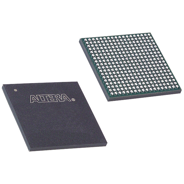
EP1C12F324C8
| Part Description |
Cyclone® Field Programmable Gate Array (FPGA) IC 249 239616 12060 324-BGA |
|---|---|
| Quantity | 606 Available (as of June 15, 2026) |

| Product Category | Field Programmable Gate Array (FPGA) |
|---|---|
| Manufacturer | Intel |
| Manufacturing Status | Obsolete |
| Manufacturer Standard Lead Time | Contact Us |
| Datasheet |
Specifications & Environmental
| Device Package | 324-FBGA (19x19) | Grade | Commercial | Operating Temperature | 0°C – 85°C | ||
|---|---|---|---|---|---|---|---|
| Package / Case | 324-BGA | Number of I/O | 249 | Voltage | 1.425 V - 1.575 V | ||
| Mounting Method | Surface Mount | RoHS Compliance | RoHS non-compliant | REACH Compliance | REACH Unknown | ||
| Moisture Sensitivity Level | 3 (168 Hours) | Number of LABs/CLBs | 1206 | Number of Logic Elements/Cells | 12060 | ||
| Number of Gates | N/A | ECCN | 3A991D | HTS Code | 8542.39.0001 | ||
| Qualification | N/A | Total RAM Bits | 239616 |
Overview of EP1C12F324C8 – Cyclone® Field Programmable Gate Array (FPGA) 324-BGA
The EP1C12F324C8 is a Cyclone® series field programmable gate array (FPGA) in a 324-ball BGA package designed for commercial applications. It delivers a balance of programmable logic, embedded memory, and flexible I/O capability suitable for data-path and interface-focused designs.
Built on the Cyclone device architecture, this device targets designers who need mid-range logic density with integrated memory, clocking resources, and multiple I/O standards to support system-level interfacing and peripheral connectivity.
Key Features
- Logic Capacity Approximately 12,060 logic elements provide the programmable fabric to implement mid-range logic, control, and datapath functions.
- Embedded Memory Approximately 0.24 Mbits of on-chip RAM (239,616 total RAM bits) for FIFOs, buffering, and local data storage.
- I/O Count and Standards 249 user I/Os with family-level support for LVTTL, LVCMOS, SSTL-2, SSTL-3 and LVDS I/O standards, enabling interface flexibility for diverse peripherals and memory.
- Clocking Family documentation indicates up to two PLLs for clock multiplication and phase shifting to support multiple clock domains and timing management.
- Voltage and Thermal Core supply range 1.425 V to 1.575 V; commercial operating temperature range 0 °C to 85 °C.
- Package & Mounting 324-FBGA (19 × 19 mm) surface-mount package (324-BGA case) for compact board integration.
- Compliance RoHS compliant; commercial-grade device classification.
Typical Applications
- Data-path and Bridge Logic Implement mid-density datapath processing, protocol bridging, and glue logic where integrated memory and flexible I/O simplify board design.
- Memory Interface Control Supports external memory interfacing scenarios referenced by the Cyclone family, including DDR SDRAM and other synchronous memory types for buffering and system memory control.
- High-speed Serial and Parallel I/O Use LVDS-capable I/O and standard parallel interfaces to connect high-speed sensors, serializers/deserializers, or peripheral buses.
- Clock Domain Management On-chip PLLs enable multi-clock designs requiring clock multiplication, phase shifting, or clock distribution across logic blocks.
Unique Advantages
- Balanced Logic and Memory Combines roughly 12k logic elements with ~0.24 Mbits of embedded RAM to support control-intensive and data-buffering functions in a single device.
- Flexible I/O Support High I/O count and support for multiple I/O standards let you interface to a wide range of peripherals and memory technologies without external translators.
- Integrated Clocking On-chip PLL resources help manage multiple clock domains and simplify timing closure for system designs.
- Compact Surface-Mount Package 324-FBGA (19 × 19 mm) package allows dense board designs while keeping a high I/O count accessible.
- Commercial-Grade Operating Range Specification for 0 °C to 85 °C operation aligns with general-purpose commercial applications.
- RoHS Compliant Meets RoHS requirements for use in regulated assemblies.
Why Choose EP1C12F324C8?
The EP1C12F324C8 provides a practical mid-range FPGA option for designers needing a compact, programmable platform with a solid mix of logic, embedded memory, and a broad complement of I/O. Its Cyclone architecture delivers integration suitable for data-path handling, memory interfacing, and multi-clock systems while fitting into space-constrained board layouts via the 324-FBGA package.
This device is ideal for commercial-product development where predictable operating temperature and supply ranges, along with RoHS compliance and family-level support for common I/O standards and clocking features, contribute to scalable designs and streamlined integration.
Request a quote today for pricing and availability, or submit your requirements to receive a tailored response for procurement and lead-time information.


Date Founded: 1968
Headquarters: Santa Clara, California, USA
Employees: 130,000+
Revenue: $54.23 Billion
Certifications and Memberships: ISO9001:2015, ISO14001:2015, ISO17025:2017, ISO27001:2022, ISO45001:2018, ISO50001:2018


