
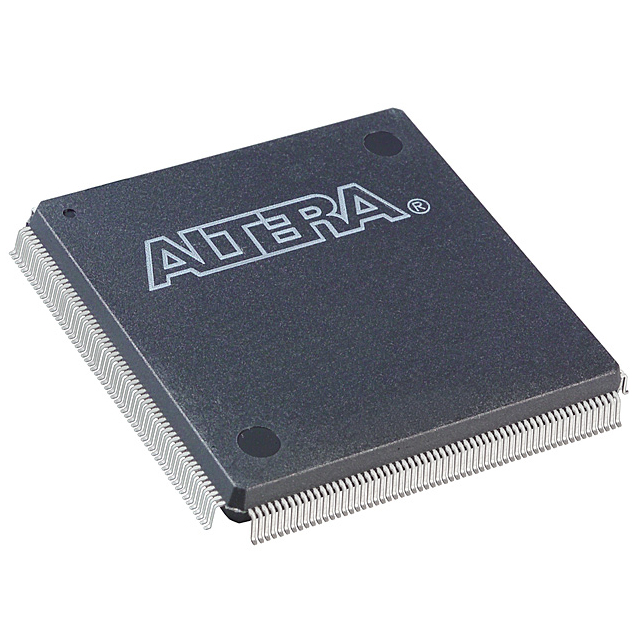
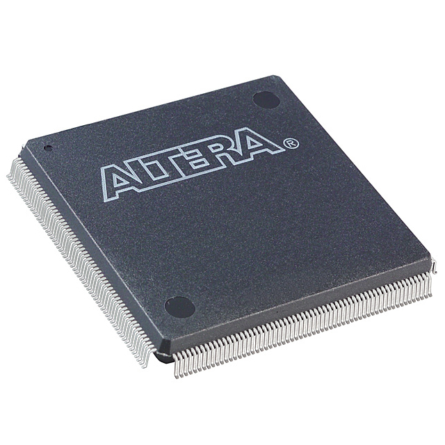
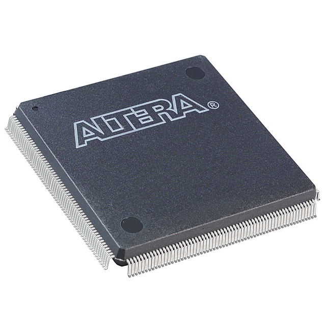
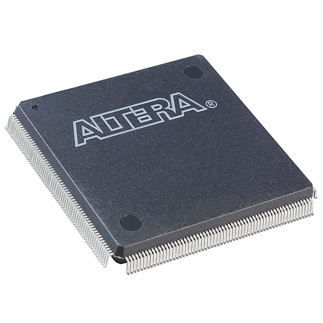
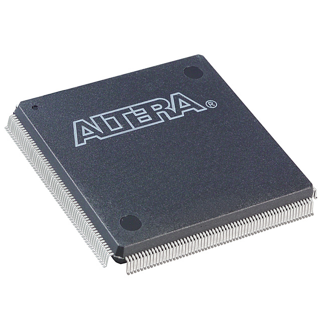
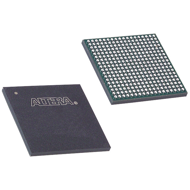
EP1C12Q240C8
| Part Description |
Cyclone® Field Programmable Gate Array (FPGA) IC 173 239616 12060 240-BFQFP |
|---|---|
| Quantity | 72 Available (as of October 8, 2026) |
| Product Category | Field Programmable Gate Array (FPGA) |
|---|---|
| Manufacturer | Intel |
| Manufacturing Status | Obsolete |
| Manufacturer Standard Lead Time | Contact Us |
| Datasheet |
Specifications & Environmental
| Device Package | 240-PQFP (32x32) | Grade | Commercial | Operating Temperature | 0°C – 85°C | ||
|---|---|---|---|---|---|---|---|
| Package / Case | 240-BFQFP | Number of I/O | 173 | Voltage | 1.425 V - 1.575 V | ||
| Mounting Method | Surface Mount | RoHS Compliance | RoHS non-compliant | REACH Compliance | REACH Unknown | ||
| Moisture Sensitivity Level | 3 (168 Hours) | Number of LABs/CLBs | 1206 | Number of Logic Elements/Cells | 12060 | ||
| Number of Gates | N/A | ECCN | 3A991D | HTS Code | 8542.39.0001 | ||
| Qualification | N/A | Total RAM Bits | 239616 |
Overview of EP1C12Q240C8 – Cyclone® Field Programmable Gate Array (FPGA) IC 173 239616 12060 240-BFQFP
The EP1C12Q240C8 is an Intel Cyclone® family FPGA providing a balance of logic capacity, on-chip memory, and I/O for cost-conscious data-path designs. It is built on the Cyclone architecture and the Cyclone family data describes a 1.5‑V, 0.13‑µm all‑layer copper SRAM process and device-level features appropriate for embedded logic, clocking and memory interfacing.
Targeted at commercial-grade applications, this device delivers 12,060 logic elements, approximately 0.24 Mbits of embedded memory, two PLLs, and 173 user I/O in a 240‑pin QFP‑style package, with a recommended supply range of 1.425 V to 1.575 V and an operating temperature range of 0 °C to 85 °C.
Key Features
- Core capacity — 12,060 logic elements for implementing medium-density combinational and sequential logic functions.
- Embedded memory — Total on-chip RAM of 239,616 bits (approximately 0.24 Mbits) to support FIFOs, buffering and data-path storage.
- Clocking resources — Device-level support includes two phase-locked loops (PLLs) for clock multiplication and phase adjustment.
- I/O — 173 user I/O pins provided for interfacing to peripherals and external devices; package and pinout support surface-mount PCB assembly.
- Power and supply — Nominal device supply specified in the range of 1.425 V to 1.575 V.
- Package and mounting — 240‑pin BFQFP package case; supplier device package listed as 240‑PQFP (32×32). Surface-mount mounting type.
- Operating range — Commercial grade operation from 0 °C to 85 °C.
- Regulatory — RoHS compliant.
- Cyclone family features — The Cyclone family supports features such as DDR memory interfacing, LVDS I/O, and PCI signaling standards as described in the Cyclone family datasheet.
Typical Applications
- Data-path processing — Use the device's logic density and embedded RAM for mid-range packet processing, protocol bridging, or stream buffering tasks.
- Memory interface control — Leverage on-chip memory and the family’s DDR interface capabilities for interfacing to external SDRAM/DDR memories and FCRAM.
- Custom peripheral glue logic — Implement user-defined interfaces and protocol conversion between ASSP/ASIC devices and system controllers.
- Clocking and timing control — Employ the device PLLs for clock multiplication, distribution and phase-shifting in multi-clock systems.
Unique Advantages
- Balanced logic and memory — 12,060 logic elements paired with ~0.24 Mbits of RAM provide a flexible platform for combined control and data buffering tasks.
- Integrated clocking — Two PLLs on-chip reduce external clocking complexity and help centralize timing control within the FPGA.
- Compact surface-mount package — 240‑pin BFQFP/PQFP packaging enables higher I/O density while remaining compatible with standard surface-mount assembly processes.
- Commercial-temperature rating — 0 °C to 85 °C operation suitable for general-purpose embedded and consumer applications.
- RoHS compliant — Meets lead-free material requirements for environmentally conscious designs.
Why Choose EP1C12Q240C8?
The EP1C12Q240C8 combines a mid-range logic element count with meaningful on-chip RAM and integrated PLL resources, making it well suited for designers who need a compact, commercially rated FPGA for data-path, interface, and control tasks. Its voltage supply window and package options accommodate common board-level power and assembly practices.
For teams building cost-sensitive embedded systems that require programmable logic, memory buffering and flexible I/O, this Cyclone device offers a verified family architecture and an established development ecosystem, delivering scalability and long-term design support consistent with Cyclone family documentation.
If you would like pricing, lead-time, or availability information for EP1C12Q240C8, request a quote or submit an inquiry to begin the procurement process.





















Date Founded: 1968
Headquarters: Santa Clara, California, USA
Employees: 130,000+
Revenue: $54.23 Billion
Certifications and Memberships: ISO9001:2015, ISO14001:2015, ISO17025:2017, ISO27001:2022, ISO45001:2018, ISO50001:2018


