
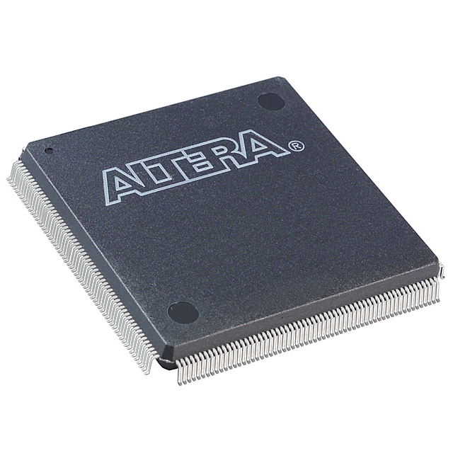
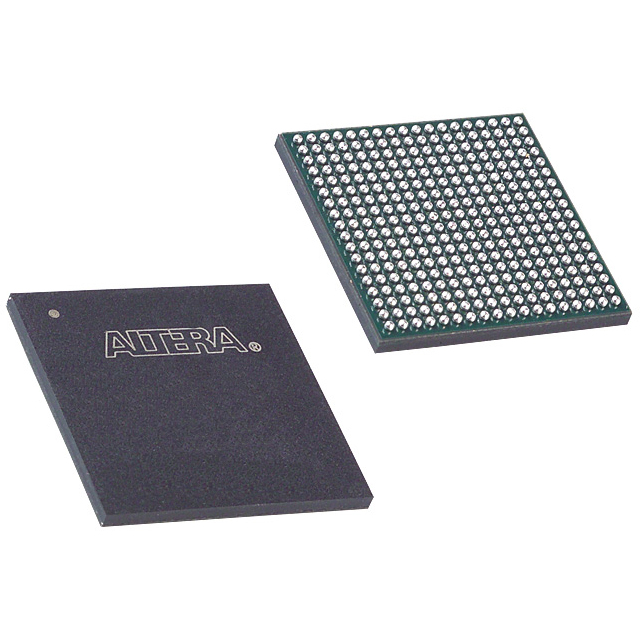
EP1C20F324C6
| Part Description |
Cyclone® Field Programmable Gate Array (FPGA) IC 233 294912 20060 324-BGA |
|---|---|
| Quantity | 989 Available (as of June 15, 2026) |

| Product Category | Field Programmable Gate Array (FPGA) |
|---|---|
| Manufacturer | Intel |
| Manufacturing Status | Obsolete |
| Manufacturer Standard Lead Time | Contact Us |
| Datasheet |
Specifications & Environmental
| Device Package | 324-FBGA (19x19) | Grade | Commercial | Operating Temperature | 0°C – 85°C | ||
|---|---|---|---|---|---|---|---|
| Package / Case | 324-BGA | Number of I/O | 233 | Voltage | 1.425 V - 1.575 V | ||
| Mounting Method | Surface Mount | RoHS Compliance | RoHS non-compliant | REACH Compliance | REACH Unknown | ||
| Moisture Sensitivity Level | 3 (168 Hours) | Number of LABs/CLBs | 2006 | Number of Logic Elements/Cells | 20060 | ||
| Number of Gates | N/A | ECCN | 3A991D | HTS Code | 8542.39.0001 | ||
| Qualification | N/A | Total RAM Bits | 294912 |
Overview of EP1C20F324C6 – Cyclone® Field Programmable Gate Array (FPGA) IC 233 294912 20060 324-BGA
The EP1C20F324C6 is a Cyclone® family SRAM-based FPGA in a 324-ball FBGA package, delivering 20,060 logic elements and approximately 294,912 bits of embedded memory for data-path and system interfacing applications. The device implements a 1.5-V, 0.13-µm all-layer copper SRAM process and is positioned for commercial-grade designs requiring flexible I/O, on-chip clocking, and a compact surface-mount package.
Typical use cases include data-path processing, memory interface logic, and system glue where a balance of logic density, embedded RAM, and mixed I/O support is required.
Key Features
- Logic Capacity Provides 20,060 logic elements to implement medium-complexity combinational and sequential logic.
- Embedded Memory Approximately 294,912 bits of on-chip RAM for FIFOs, buffers, and small lookup tables.
- I/O Density 233 user I/O pins to support broad peripheral and bus connectivity in a single device.
- Configurable I/O Standards Device family supports LVTTL, LVCMOS, SSTL-2, SSTL-3 and high-speed LVDS interfaces (LVDS up to 640 Mbps and low-speed LVDS options), enabling a range of signaling choices for system integration.
- Memory and System Interfaces Architected to support external memories and high-bandwidth interfaces including DDR SDRAM and PCI standards (66/33 MHz, 64-/32-bit as supported by the Cyclone family).
- On-chip Clocking Up to two PLLs per device provide clock multiplication and phase shifting for flexible clock management.
- Package and Mounting 324-FBGA (19 × 19) surface-mount package for compact board-level integration.
- Power Nominal core supply voltage range: 1.425 V to 1.575 V.
- Operating Grade Commercial grade with an operating temperature range of 0 °C to 85 °C.
- Compliance RoHS compliant.
Typical Applications
- Data-Path Processing Implements custom datapath logic, protocol conversion, and packet handling using the device’s logic elements and embedded RAM.
- Memory Interface Controllers Used for DDR SDRAM and SDRAM interfaces where on-chip PLLs and supported I/O standards simplify timing and signaling.
- High-Speed I/O and Serialization Leverages LVDS support and numerous I/O pins for high-speed links, video, or sensor data aggregation.
- PCI and System Glue Acts as a bridge or interface logic for PCI-based subsystems and peripheral expansion leveraging supported PCI signaling modes.
Unique Advantages
- Highly integrated logic and memory: 20,060 logic elements combined with ~294,912 bits of embedded RAM reduce the need for external components and simplify board-level design.
- Flexible I/O support: Broad support for LVTTL, LVCMOS, SSTL, and LVDS lets you match signaling to diverse peripherals and memory interfaces.
- Compact FBGA package: 324-FBGA (19 × 19) enables high I/O count in a compact footprint for space-constrained PCBs.
- On-chip clock management: Up to two PLLs provide clock multiplication and phase shifting to meet complex timing requirements without extra silicon.
- Commercial-grade reliability: Rated for 0 °C to 85 °C operation and RoHS compliant for mainstream commercial deployments.
- Ecosystem support: Cyclone family devices are supported by Altera® MegaCore® functions and Quartus® II software for IP integration and device migration across family densities.
Why Choose EP1C20F324C6?
The EP1C20F324C6 delivers a practical balance of logic capacity, embedded memory, and flexible I/O in a compact 324-FBGA package, suited to commercial designs that require on-chip memory, clocking, and a variety of signaling standards. With two on-chip PLLs and support for common memory and I/O protocols, this Cyclone FPGA simplifies implementation of data-path and interface functions while keeping board-level BOM effort lower.
This device is a good fit for engineers and system designers building medium-complexity FPGA-based controllers, protocol bridges, or memory interface logic who need a commercially rated, RoHS-compliant FPGA with established software and IP support.
If you would like pricing, lead-time, or availability information for EP1C20F324C6, request a quote or contact sales to discuss your requirements and procurement options.


Date Founded: 1968
Headquarters: Santa Clara, California, USA
Employees: 130,000+
Revenue: $54.23 Billion
Certifications and Memberships: ISO9001:2015, ISO14001:2015, ISO17025:2017, ISO27001:2022, ISO45001:2018, ISO50001:2018


